AMD
P R E L I M I N A R Y
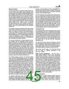
4 X TSCLK
TXS
TGAP1 X TBCLK
+ 2 X TSCLK
TGAP4 X TBCLK
+ 2 X TSCLK
T1
T2
TGAP2 X TBCLK
+ 2 X TSCLK
TGAP3 X TBCLK
+ 2 X TSCLK
2 X TSCLK
2 X TSCLK
T3
3 X TSCLK
7 X TSCLK
O_TX
TXP_ON
TXDATA
HDB X TBCLK
DRB X TBCLK
1st
Data Bit
Last
Data Bit
TX default bit
TX default bit
TSCLK = TCLKIN when
CLKGT20 = 0
TBCLK = TSCLK X 20
20183B-7
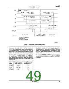
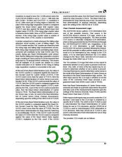
Figure 1. Transmitter Power Ramp Control
The values HDR, DRB, TGAP1, TGAP2, TGAP3, and
TGAP4 are programmable values that are stored in
TCR register locations TCR0, TCR5, and TCR6. All
other timings in the diagram are fixed with the values in-
dicated. The CLKGT20 control bit is located in MIR9[7].
Note that the TXCMD, TXPE, and TXMOD bits of TIR11
may also affect the values of the TXCMD, TXPE, and
TXMOD pins. See the individual descriptions of these
pins in the Multi-Function Pin section of this document
for more detail.
The timing of the five internal signals can be applied to
the external pins TXCMD, TXPE, and TXMOD in
either of two ways, depending upon the value pro-
grammed into the RCEN bit of TIR11 as shown in the
following table:
The polarity of TXMOD and TXPE are programmable. A
separate TXCMD signal (inverse polarity to TXCMD)
is available.
Pin
Timing Reference Timing Reference
Name
When RCEN=0
When RCEN=1
TXCMD
TXPE
O_TX
T1
T2
T3
TXP_ON
T3
TXMOD
Am79C930
49

 AMD [ AMD ]