AMD
P R E L I M I N A R Y
selection of antennas. If automatic antenna selection is
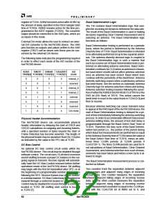
Transceiver Attachment Interface Unit
not used, then the desired antenna selection is accom-
plished through the setting of appropriate bits in one of
the TIR registers.
The TAI Unit includes the following subfunctions:
TAI register set
TX FIFO
TX FIFO
TX data serialization
TX CRC32 generation
TX CRC8 generation
TX status reporting
RX preamble and Start of Frame detection
RX data deserialization
RX FIFO
RX CRC32 checking
RX CRC8 checking
RX status reporting
Bit ordering
The TAI contains individual FIFOs for RX and TX opera-
tions. The TX FIFO holds a maximum of 8 bytes. The TX
FIFO indicates a “not full” state by signaling a request for
data on the DRQ1 input of the 80188 embedded core.
The DRQ1 output of the TAI subunit is active if the TX
FIFO condition is met, regardless of the state of the TXS
bit of TIR8. TX FIFO DMA activity is prevented by dis-
abling the DMA1 controller in the 80188.
The TX FIFO holds a maximum of 8 bytes of data. Actual
TX FIFO byte count can be read from TIR9. Preamble
and Start of Frame Delimiter and any necessary PHY
subunit header information must be assembled by the
80188 core firmware and then loaded into the TX FIFO
for inclusion in the TX frame. The TAI subunit has
no built in capabilities for preamble, SFD, or PHY
header generation.
RSSI A/D circuit
Physical Header Accommodation
Encryption/decryption support
Data Scrambling
DC Bias Control
Baud Determination logic
CCA circuit
Antenna diversity logic
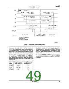
TX Power Ramp Control
The Am79C930 device includes state-controlled output
signals that may be used to perform transceiver power
sequencing. For transceivers that create their own
transmit power sequencing, a single input signal (CTS)
is provided to allow for smooth synchronization between
the Am79C930 device and the transceiver.
The TAI provides the necessary functionality to directly
connect to a variety of possible transceiver interface
styles. In the PCMCIA mode of operation, 24 pins are di-
rectly controllable through register access by the device
driver and the 80188 core firmware. These 24 pins may
be combined with the fixed function pins of the network
interface to create a customer-specific network inter-
face. In the ISA Plug and Play mode of operation, the
number of programmable pins is reduced to 10, while
the fixed function pins remain unchanged.
Am79C930-based TX Power Ramp Control — The
following is the description of the Am79C930 device’s
state-controlled output signals. The subsequent
section is a description of the CTS input signal and its
intended use.
The TAI is logically located on the Am79C930 memory
interface bus as a slave-only device. The TAI contains
64 registers that are used to configure operational pa-
rameters, to communicate commands, to pass data,
and to pass status. Thirty-two of the registers are di-
rectly accessible to the 80188 core and to the system
interface. These 32 registers are labeled TAI Interface
Registers (TIR). An additional 32 TAI registers are indi-
rectly accessible through an address and data port in
the TIR register set. These 32 registers are labeled TAI
Configuration Registers (TCR).
Once the TX start command has been issued to the TAI
by the 80188 core firmware (TXS bit of TIR8), a
sequence of transceiver enable signals will be gener-
ated in order to ramp up the power to the various sec-
tions of the transceiver (i.e., TXCMD, TXPE, TXMOD).
Once the final enable signal has been sent to the trans-
ceiver, the TAI will begin to remove data from the TX
FIFO. As each byte of data is removed from the TX
FIFO, the TAI subunit will serialize the byte and send the
individual bits of the data out the TXDATA pin at the
specified data transmission rate.
Data transfers from the RX FIFO are requested through
the internal 80188 core input DRQ0. Data transfers to
the TX FIFO are requested through the internal 80188
core input DRQ1. Interrupts from the TAI are requested
through the internal 80188 core input INT0.
Timing for the transmit ramp up and ramp down se-
quence is generated from 5 internal signals whose tim-
ing relationships may be directly controlled by register
programming (TCR5, TCR6). The following diagram il-
lustrates the relationships among the five internal sig-
nals and the registers that control them.
The TAI supplies an antenna select pin to allow for se-
lection between two possible antennas. The Am79C930
device has provision for both automatic and manual
48
Am79C930

 AMD [ AMD ]