P R E L I M I N A R Y
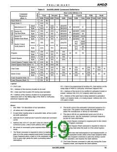
5 shows the address and data requirements for the
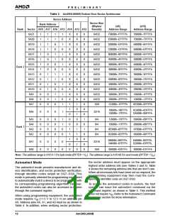
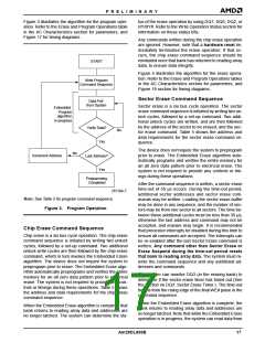
Autoselect Command Sequence
byte program command sequence.
The autoselect command sequence allows the host
system to access the manufacturer and devices codes,
and determine whether or not a sector is protected.
Table 5 shows the address and data requirements. This
method is an alternative to that shown in Table 4, which
is intended for PROM programmers and requires VID
on address pin A9. The autoselect command sequence
may be written to an address within a bank that is either
in the read or erase-suspend-read mode. The autose-
lect command may not be written while the device is
actively programming or erasing in the other bank.
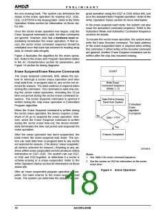
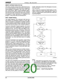
When the Embedded Program algorithm is complete,
that bank then returns to reading array data and ad-
dresses are no longer latched. The system can deter-
mine the status of the program operation by using DQ7,
DQ6, or RY/BY#. Note that while the Embedded Pro-
gram operation is in progress, the system can read
data from the non-programming bank. Refer to the
Write Operation Status section for information on these
status bits.
Any commands written to the device during the Em-
bedded Program Algorithm are ignored. Note that a
hardware reset immediately terminates the program
operation. The program command sequence should be
reinitiated once that bank has returned to reading array
data, to ensure data integrity.
The autoselect command sequence is initiated by first
writing two unlock cycles. This is followed by a third
write cycle that contains the bank address and the au-
toselect command. The addressed bank then enters
the autoselect mode. The system may read at any ad-
dress within the same bank any number of times with-
out initiating another autoselect command sequence:
Programming is allowed in any sequence and across
sector boundaries. A bit cannot be programmed
from “0” back to a “1.” Attempting to do so may cause
that bank to set DQ5 = 1, or cause the DQ7 and DQ6
status bits to indicate the operation was successful.
However, a succeeding read will show that the data is
still “0.” Only erase operations can convert a “0” to a
“1.”
■ A read cycle at address (BA)XX00h (where BA is
the bank address) returns the manufacturer code.
■ A read cycle at address (BA)XX01h in word mode
(or (BA)XX02h in byte mode) returns the device
code.
■ A read cycle to an address containing a sector ad-
dress (SA) within the same bank, and the address
02h on A7–A0 in word mode (or the address 04h on
A6–A-1 in byte mode) returns 01h if the sector is
protected, or 00h if it is unprotected. Refer to Tables
2 and 3 for valid sector addresses.
Unlock Bypass Command Sequence
The unlock bypass feature allows the system to pro-
gram bytes or words to a bank faster than using the
standard program command sequence. The unlock by-
pass command sequence is initiated by first writing two
unlock cycles. This is followed by a third write cycle
containing the unlock bypass command, 20h. That
bank then enters the unlock bypass mode. A two-cycle
unlock bypass program command sequence is all that
is required to program in this mode. The first cycle in
this sequence contains the unlock bypass program
command, A0h; the second cycle contains the program
address and data. Additional data is programmed in
the same manner. This mode dispenses with the initial
two unlock cycles required in the standard program
command sequence, resulting in faster total program-
ming time. Table 5 shows the requirements for the com-
mand sequence.
The system may continue to read array data from the
other bank while a bank is in the autoselect mode. To
exit the autoselect mode, the system must write the
reset command to return both banks to reading array
data. If a bank enters the autoselect mode while erase
suspended, a reset command returns that bank to the
erase-suspend-read mode. A subsequent Erase
Resume command returns the bank to the erase oper-
ation.
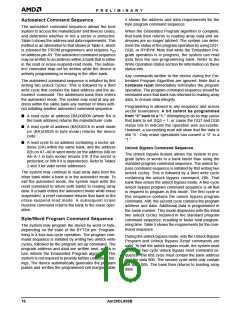
Byte/Word Program Command Sequence
The system may program the device by word or byte,
depending on the state of the BYTE# pin. Program-
ming is a four-bus-cycle operation. The program com-
mand sequence is initiated by writing two unlock write
cycles, followed by the program set-up command. The
program address and data are written next, which in
turn initiate the Embedded Program algorithm. The
system is not required to provide further controls or tim-
ings. The device automatically generates the program
pulses and verifies the programmed cell margin. Table
During the unlock bypass mode, only the Unlock Bypass
Program and Unlock Bypass Reset commands are
valid. To exit the unlock bypass mode, the system must
issue the two-cycle unlock bypass reset command se-
quence. The first cycle must contain the bank address
and the data 90h. The second cycle need only contain
the data 00h. The bank then returns to reading array
data.
16
Am29DL800B

 AMD [ AMD ]