AMD
The circuitry that handles the Sync Commands or Sync Bytes generates several signals.
The CMND0, CLR_CNTR, Sync and PCO are the signals that are generated by Sync
Command logic. The CLR_CNTR signal is generated from the CMND0 and the CSTRB
signal which signify a Sync Command has been received. CLR_CNTR clears the
controller and then is latched by the rising edge of the Receiver CLK to form the Sync
signal. The Sync signal then generates an active PCO signal. The CLKOUT is then
driven High on the following rising edge of CLK if CLK4 has not already driven the
CLKOUT signal High. The Sync Command only clocks out the data when it is received
before the fourth byte of data has been received. In all other cases, the data is clocked
out by the logic involved with the fourth state of the controller. The Sync Commands that
follow this Sync Command hold the CLKOUT signal High to effectively hold the control-
ler circuitry in a constant state of reset with no change to the output data.
Bu ffe rin g :
The buffering of signals should also be considered for this design. In this example, the
data outputs from the TAXI Receiver drive the first column of four low power registers.
This design does not exceed the driving capacity of the Receiver, but if different parts
are used, load calculations should be redone.
This system should work with any standard logic, although logic families should not be
mixed unless timing considerations have been made. This particular example uses low
power Schottky devices with relatively fast low power output registers.
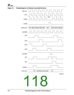
TIMING CONS IDERATIONS
Some critical timing considerations must be met to ensure the proper operation of this
design. In order to capture the DSTRB signal, the timing of DSTRB going active and the
rising edge of the CLKx signals from the controller must agree with the setup and hold
times of the first column of registers. To ensure capture of Sync Commands, the
CLR_CNTR signal becoming active and the rising edge of the Receiver CLK must agree
with the setup and hold times of the Sync flip flop. To prevent glitches on the CLKx
signals and the potential capture of incorrect data, the timing between CLK_CNTR rising
and CLR_CNTR becoming active must be considered, CLR_CNTR needs to become
active at a time before CLK_CNTR can effect the output of CLKx. The timing diagram is
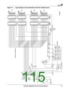
shown in Figure 16.
Figure 16 shows the timing of the system where one Sync Command is received
between data blocks being received. The premature Sync Command is not shown, but
can be derived by following the given timing diagram and known responses of the logic
given in Figure 15.
UP GRADE NOTES
Co m m a n d Lin e Ha n d lin g :
To add the capability to receive Commands in this design, only a few additions are
necessary. Since this design uses 8-bit data mode, 4-bit commands can be used. It will
be necessary to add command storage registers four bits wide as well as command
output registers four bits wide to output these Command lines correctly. The CLKx
signals as well as the CLKOUT signals for the existing registers need to be connected to
these new registers. The CLKx signals may need to be buffered to meet fanout limita-
tions of the controller circuitry.
Co n t ro l S ig n a ls :
The signals that need to be output by the new features do not add to the logic. The
circuitry to capture the CSTRB signal is already designed into the system. The DSTRB
signal can be used as a CSTRB indicator, active Low, as well as a DSTRB indicator,
112
TAXIchip Integrated Circuits Technical Manual

 AMD [ AMD ]