AMD
TAXI Technical Information Publication #89-13
S u b je c t : De m u x in g A TAXIc h ip Re c e ive r Ou t p u t t o Mu lt i-Byt e Wo rd s
Qu e s t io n :
How can a single TAXI Receiver be used to receive multi-byte words?
An s w e r:
INTRODUCTION
For systems that require data reception wider than a single byte, a single TAXI Receiver
can be used to cascade the multiple bytes. This operation allows the data to be
demultiplexed from a single serial link and used by an external system.
In the following example, data is captured sequentially and output in the form of four
8-bit words. Commands, which can also be transmitted are not used in this example in
order to clarify the basics of the technique. Some simple modifications to include
commands will be presented at the end of this technical note.
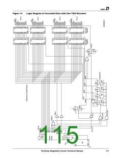
The circuit shown in Figure 14 illustrates the logic configuration that has been built and
tested in the laboratory using nominal commercial parts. The circuit handles blocks of
data typically ranging from four bytes to 64K bytes.
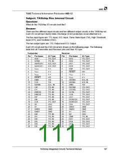
The TAXI Receiver converts the serial information that is received by the SERIN+/–
inputs to the data information that is output by the D0–D7 Data pins, C0–C3 Command
pins, and the DSTRB, CSTRB, and VLTN pins. This data information output by the
single receiver is used by the controller to capture the incoming data and output it four
bytes at a time.
FUNCTIONAL DES CRIP TION
Co n t ro lle r Circ u it :
The controller consists of a shift register constructed of four D flip-flops and a 3-input
NOR gate. The shifter is loaded with a 1 that progresses through the flip-flops sequen-
tially clocking the first column of four registers which capture the incoming data. When
the 1 is shifted through the fourth flip-flop, it raises the PCO signal for the CLKOUT D
flip-flop. On the following rising edge of the /CLK signal the bytes of cascaded data are
simultaneously clocked out through the second column of four registers that buffer the
cascaded data to the outside system.
Co n t ro lle r Clo c k :
The clock for the controller circuit is generated by OR-ing DSTRB and CSTRB. This
ensures that the DSTRB signal is captured for output to the external system. These signals
also prepare the way for a simple upgrade to allow the use of commands (explained later).
S yn c Co m m a n d s :
When not receiving blocks of data, Sync Commands (bytes) are received which keeps
the TAXI Receiver locked onto the correct byte rate and byte boundaries. This ensures
proper capture of the data at the beginning of the next block. In addition, before a block
of data is to be sent, a Sync Command must be received to reset the counter to the
proper byte alignment and initialize the system. The Sync Commands are sent by
default in the system because they are automatically inserted whenever a byte time
passes without a STRB (no data to send) pulse at the transmitter. It is important to note
that the Receiver generates a CSTRB and outputs zeros on the Command lines when a
Sync Command is received.
110
TAXIchip Integrated Circuits Technical Manual

 AMD [ AMD ]