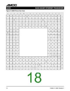
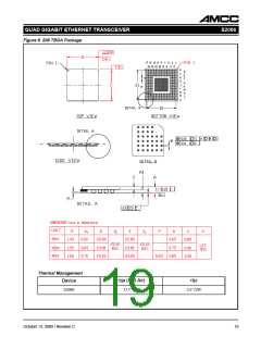
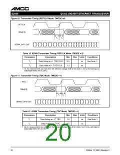
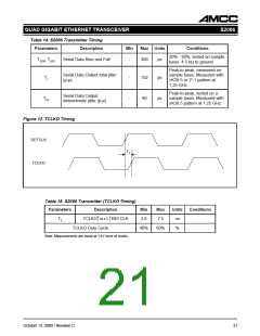
S2066
QUAD GIGABIT ETHERNET TRANSCEIVER
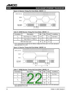
Figure 13. Receiver Timing (Full Clock Mode, CMODE = 1)
SERIAL DATA IN
RBC0x
RBC1x
DOUTx[0:9],
COM_DETx
T4
T5
Table 16. S2066 Receiver Timing (Full Clock Mode, CMODE = 1)
Parameters
Description
Min
2.75
2.0
Max Units
Conditions
T4
T5
Data Setup w.r.t. RBC1x
Data Hold w.r.t. RBC1x
-
-
ns
ns
%
See Note 1.
RBC1/0x Duty Cycle
40
60
1. All AC measurements are made from the reference voltage level of the clock (1.4V) to the valid input or
output data levels (.8V or 2.0V).
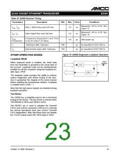
Figure 14. Receiver Timing (Half Clock Mode, CMODE = 0)
SERIAL DATA IN
RBC0x
RBC1x
DOUTx[0:9],
COM_DETx
T6
T7
T6
T7
T8
Table 17. S2066 Receiver Timing (Half Clock Mode, CMODE = 0)
Parameters
Description
Min
2.5
2.0
Max Units
Conditions
T6
T7
Data Setup w.r.t. RBC1/0x
Data Hold w.r.t. RBC1/0x
-
-
ns
ns
See Note 1.
Time from RBC1x rise to
RBC0x rise
T8
7.8
8.82
ns
RBC1/0x Duty Cycle
40
60
%
1. All AC measurements are made from the reference voltage level of the clock (1.4V) to the valid input or
output data levels (.8V or 2.0V).
22
October 13, 2000 / Revision C

 AMCC [ APPLIED MICRO CIRCUITS CORPORATION ]