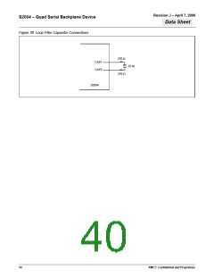
Revision J – April 7, 2006
S2004 – Quad Serial Backplane Device
Data Sheet
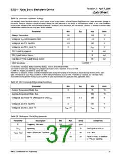
Table 24. Absolute Maximum Ratings
The following are the absolute maximum stress ratings for the S2004 device. Stresses beyond those listed may cause permanent damage to
the device. Absolute maximum ratings are stress ratings only, and operation of the device at the maximums stated, or any other conditions
beyond those indicated in the “Recommended Operating Conditions” of the document, are not inferred. Exposure to absolute maximum rating
conditions for extended periods may affect device reliability.
Parameter
Min
-65
Typ
Max
150
Units
°C
Storage Temperature
Voltage on VDD with Respect to GND
Voltage on any TTL Input Pin
Voltage on any PECL Input Pin
TTL Output Sink Current
-0.5
+5.0
V
-0.5
0
3.47
VDD
8
V
V
mA
mA
mA
TTL Output Source Current
High Speed PECL Output Source Current
ESD Sensitivity
8
25
Over 500 V
Electrostatic Discharge (ESD) Sensitivity Rating - Human Body Model (HBM):
The S2004 is rated to the following ESD voltages based upon JEDEC standard: JESD22-A114-B
CLASS 1B - All pins are rated at or above 500 volts.
Adherence to standards for ESD protection should be taken during the handling of the devices to ensure that the devices are not dam-
aged. The standards to be used are defined in ANSI standard ANSI/ESD S20.20-1999, “Protection of Electrical and Electronic Parts,
Assemblies and Equipment.” Contact your local FAE or sales representative for applicable ESD application notes.
Table 25. Recommended Operating Conditions
Parameter
Ambient Temperature Under Bias
Min
Typ
Max
70
Units
°C
0
Junction Temperature Under Bias
130
3.47
°C
Voltage on any Power Pin with respect to GND/VSS
3.13
3.3
V
Voltage on any TTL Input Pin
Voltage on any PECL Input Pin
0
3.47
VDD
V
V
VDD -2V
Table 26. Reference Clock Requirements
Parameter
Description
Min
Max
Units
Conditions
FT
Frequency Tolerance
-100
+100
ppm
TD1-2
TRCR, TRCF
—
Symmetry
40
60
2
%
ns
ps
Duty Cycle at 50% pt.
20% -80%.
REFCLK Rise and Fall Time
Jitter
80
Peak-to-Peak, to maintain
≥ 77% eye opening.
AMCC Confidential and Proprietary
37

 AMCC [ APPLIED MICRO CIRCUITS CORPORATION ]