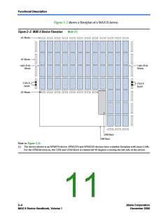
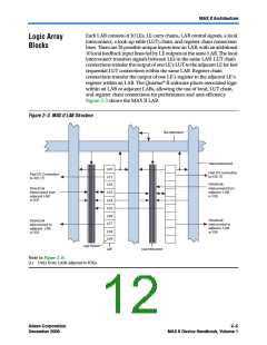
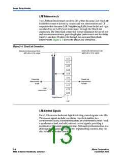
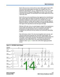
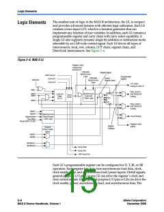
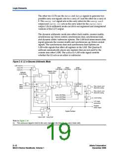
Logic Elements
The smallest unit of logic in the MAX II architecture, the LE, is compact
and provides advanced features with efficient logic utilization. Each LE
contains a four-input LUT, which is a function generator that can
implement any function of four variables. In addition, each LE contains a
programmable register and carry chain with carry select capability. A
single LE also supports dynamic single bit addition or subtraction mode
selectable by an LAB-wide control signal. Each LE drives all types of
interconnects: local, row, column, LUT chain, register chain, and
DirectLink interconnects. See Figure 2–6.
Logic Elements
Figure 2–6. MAX II LE
Register chain
routing from
previous LE
LAB-wide
Synchronous
Register Bypass
LAB Carry-In
Load
Programmable
Register
LAB-wide
Synchronous
Clear
Packed
Register Select
Carry-In1
Carry-In0
addnsub
data1
LUT chain
routing to next LE
Row, column,
and DirectLink
routing
PRN/ALD
data2
data3
Synchronous
Load and
Clear Logic
Look-Up
Table
(LUT)
Carry
Chain
D
Q
ADATA
data4
ENA
CLRN
Row, column,
and DirectLink
routing
labclr1
labclr2
Asynchronous
Clear/Preset/
Load Logic
Local Routing
labpre/aload
Chip-Wide
Reset (DEV_CLRn)
Register chain
output
Register
Feedback
Clock &
Clock Enable
Select
labclk1
labclk2
labclkena1
labclkena2
Carry-Out0
Carry-Out1
LAB Carry-Out
Each LE’s programmable register can be configured for D, T, JK, or SR
operation. Each register has data, true asynchronous load data, clock,
clock enable, clear, and asynchronous load/preset inputs. Global signals,
general-purpose I/O pins, or any LE can drive the register’s clock and
clear control signals. Either general-purpose I/O pins or LEs can drive the
clock enable, preset, asynchronous load, and asynchronous data. The
2–8
MAX II Device Handbook, Volume 1
Core Version a.b.c variable
Altera Corporation
December 2006

 ALTERA [ ALTERA CORPORATION ]