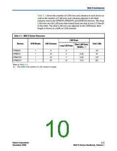
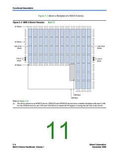
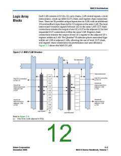
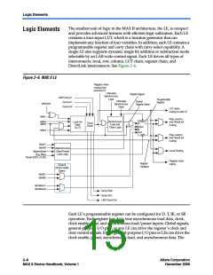
MAX II Architecture
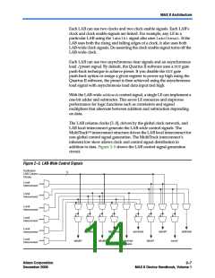
Each LAB can use two clocks and two clock enable signals. Each LAB’s
clock and clock enable signals are linked. For example, any LE in a
particular LAB using the labclk1signal also uses labclkena1. If the
LAB uses both the rising and falling edges of a clock, it also uses both
LAB-wide clock signals. De-asserting the clock enable signal turns off the
LAB-wide clock.
Each LAB can use two asynchronous clear signals and an asynchronous
load /preset signal. By default, the Quartus II software uses a NOT gate
push-back technique to achieve preset. If you disable the NOT gate
push-back option or assign a given register to power-up high using the
Quartus II software, the preset is then achieved using the asynchronous
load signal with asynchronous load data input tied high.
With the LAB-wide addnsubcontrol signal, a single LE can implement a
one-bit adder and subtractor. This saves LE resources and improves
performance for logic functions such as correlators and signed
multipliers that alternate between addition and subtraction depending
on data.
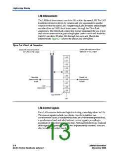
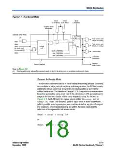
The LAB column clocks [3..0], driven by the global clock network, and
LAB local interconnect generate the LAB-wide control signals. The
TM
MultiTrack interconnect structure drives the LAB local interconnect for
non-global control signal generation. The MultiTrack interconnect’s
inherent low skew allows clock and control signal distribution in
addition to data. Figure 2–5 shows the LAB control signal generation
circuit.
Figure 2–5. LAB-Wide Control Signals
Dedicated
LAB Column
Clocks
4
Local
Interconnect
Local
Interconnect
Local
Interconnect
Local
Interconnect
Local
Interconnect
labclkena2
labclkena1
syncload
labclr2
addnsub
Local
Interconnect
labclk1
labclk2
asyncload
or labpre
labclr1
synclr
Altera Corporation
December 2006
Core Version a.b.c variable
2–7
MAX II Device Handbook, Volume 1

 ALTERA [ ALTERA CORPORATION ]