Chapter 17: Understanding and Evaluating Power in MAX II Devices
17–11
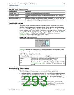
PowerPlay Early Power Estimator Inputs
Table 17–6. I/O Section Information (Part 2 of 2)
Column Heading
Description
OE %
Enter the average percentage of time that:
■ The output I/O pins are enabled.
■ Bidirectional I/O pins are outputs and enabled.
During the remaining time:
■ Output I/O pins are tri-stated.
■ Bidirectional I/O pins are inputs.
This number must be a percentage between 0% and 100%.
Load (pF)
Enter the pin loading external to the chip (pF). This parameter only applies to output and
bidirectional pins.
Pin and package capacitance is already included in the I/O model. Therefore, you only need to
include off-chip capacitance in the Load parameter.
Bank I/O Std Check
Bank Voltage Check
Routing
Indicates whether the selected I/O standard is available on the selected I/O bank or not. Not all I/O
banks can implement every I/O standard.
Indicates whether the selected I/O bank has a voltage compatible with the selected I/O standard
or not.
Represents the power dissipation due to estimated routing.
Routing power is highly dependent on placement and routing, which itself is a function of design
complexity. The values shown are representative of routing power based on experimentation on
over 100 real-world designs.
Use the Quartus II PowerPlay Power Analyzer for detailed analysis based on the routing used in
your design.
Block
Total
Represents the power dissipation due to internal and load toggling of the I/O.
Use the Quartus II PowerPlay Power Analyzer for accurate analysis based on the exact I/O
configuration of your design.
Represents the total power dissipation. The total power dissipation is the sum of the routing and
block power.
ICCINT
Represents the current drawn from the ICCINT rail. Powers internal digital circuitry and routing.
Represents the current drawn from this bank’s VCCIO rail.
ICCIO
User Comment
Enter any comments (optional entry).
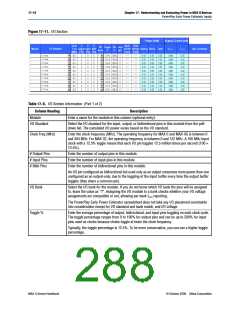
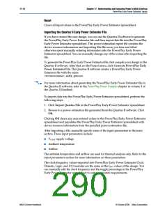
Other Input Information
There are three other buttons below the input parameters section: Set Toggle %, Reset,
and Import Quartus File, as shown in Figure 17–12.
Figure 17–12. The Three Buttons
Set Toggle %
Sets the toggle rate for the Logic Module and I/O Module.
© October 2008 Altera Corporation
MAX II Device Handbook

 ALTERA [ ALTERA CORPORATION ]