Chapter 7: Package Information
7–3
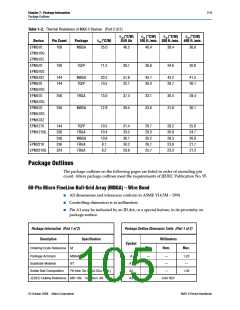
Package Outlines
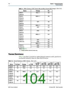
Table 7–2. Thermal Resistance of MAX II Devices (Part 2 of 2)
θJA (°C/W)
θJA (°C/W)
θJA (°C/W)
θJA (°C/W)
Device
EPM570
Pin Count
Package
θJC (°C/W)
Still Air
100 ft./min. 200 ft./min. 400 ft./min.
100
MBGA
25.0
46.5
40.4
36.6
38.4
36.8
EPM570G
EPM570Z
EPM570
100
TQFP
11.2
38.7
34.6
30.8
EPM570G
EPM570Z
EPM570
144
144
MBGA
TQFP
20.2
10.5
51.8
32.1
45.1
30.3
43.2
28.7
41.5
26.1
EPM570G
EPM570
256
256
FBGA
13.0
12.9
37.4
39.5
33.1
33.6
30.5
31.6
28.4
30.1
EPM570G
EPM570
MBGA
EPM570G
EPM570Z
EPM1270
EPM1270G
144
256
256
256
324
TQFP
FBGA
MBGA
FBGA
FBGA
10.5
10.4
10.6
8.7
31.4
33.5
36.1
30.2
29.8
29.7
29.3
30.2
26.1
25.7
28.2
26.8
28.3
23.6
23.3
25.8
24.7
26.8
21.7
21.3
EPM2210
EPM2210G
8.2
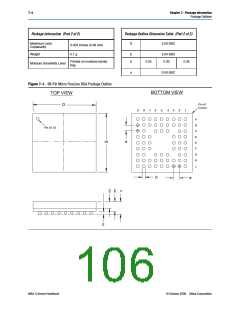
Package Outlines
The package outlines on the following pages are listed in order of ascending pin
count. Altera package outlines meet the requirements of JEDEC Publication No. 95.
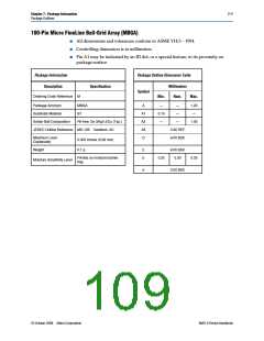
68-Pin Micro FineLine Ball-Grid Array (MBGA) – Wire Bond
■
All dimensions and tolerances conform to ASME Y14.5M – 1994
■
Controlling dimension is in millimeters
■
Pin A1 may be indicated by an ID dot, or a special feature, in its proximity on
package surface
Package Information (Part 1 of 2)
Package Outline Dimension Table (Part 1 of 2)
Description
Specification
Millimeters
Symbol
Ordering Code Reference
M
Min.
Nom.
Max.
Package Acronym
MBGA
BT
A
—
0.15
—
—
—
1.20
—
Substrate Material
A1
A2
A3
Solder Ball Composition
Pb-free: Sn:3Ag:0.5Cu (Typ.)
—
1.00
JEDEC Outline Reference MO-195 Variation: AB
0.60 REF
© October 2008 Altera Corporation
MAX II Device Handbook

 ALTERA [ ALTERA CORPORATION ]