7. Package Information
MII51007-2.1
Introduction
®
This chapter provides package information for Altera’s MAX II devices, and includes
these sections:
■
■
■
■
“Board Decoupling Guidelines” on page 7–1
“Device and Package Cross Reference” on page 7–1
“Thermal Resistance” on page 7–2
“Package Outlines” on page 7–3
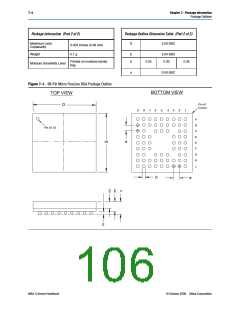
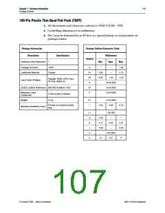
In this chapter, packages are listed in order of ascending pin count. See Figure 7–1
through 7–17.
Board Decoupling Guidelines
Decoupling requirements are based on the amount of logic used in the device and the
output switching requirements. As the number of I/O pins and the capacitive load on
the pins increase, more decoupling capacitance is required. As many as possible 0.1-
mF power-supply decoupling capacitors should be connected to the VCCand GND
pins or the VCCand GNDplanes. These capacitors should be located as close as
possible to the MAX II device. Each VCCINT/GNDINTand VCCIO/GNDIOpair should
be decoupled with a 0.1-mF capacitor. When using high-density packages, such as
ball-grid array (BGA) packages, it may not be possible to use one decoupling
capacitor per VCC/GNDpair. In this case, you should use as many decoupling
capacitors as possible. For less dense designs, a reduction in the number of capacitors
may be acceptable. Decoupling capacitors should have a good frequency response,
such as monolithic-ceramic capacitors.
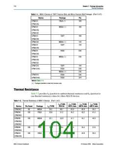
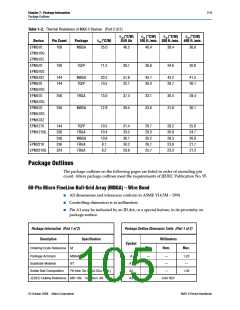
Device and Package Cross Reference
®
Table 7–1 shows which Altera MAX II devices are available in thin quad flat pack
(TQFP), FineLine BGA (FBGA), and Micro Fineline BGA (MBGA) packages.
Table 7–1. MAX II Devices in TQFP, FineLine BGA, and Micro FineLine BGA Packages (Part 1 of 2)
Device
Package
MBGA (1)
FBGA (1)
Pin
68
EPM240Z
EPM240
100
EPM240G
EPM240
MBGA (1)
100
100
EPM240G
EPM240Z
EPM240
TQFP
EPM240G
© October 2008 Altera Corporation
MAX II Device Handbook

 ALTERA [ ALTERA CORPORATION ]