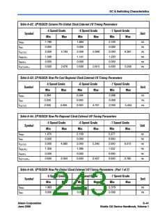
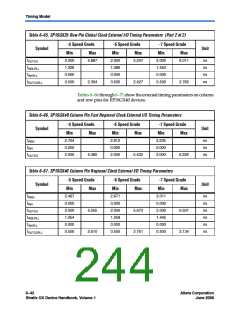
DC & Switching Characteristics
Table 6–72. Stratix GX I/O Standard Column Pin Input Delay Adders (Part 2 of 2)
-5 Speed Grade -6 Speed Grade -7 Speed Grade
I/O Standard
Unit
Min
Max
Min
Max
Min
Max
SSTL-2 class I
–70
–70
180
180
120
120
70
–74
–74
189
189
126
126
73
–86
–86
217
217
144
144
83
ps
ps
ps
ps
ps
ps
ps
ps
SSTL-2 class II
SSTL-18 class I
SSTL-18 class II
1.5-V HSTL class I
1.5-V HSTL class II
1.8-V HSTL class I
1.8-V HSTL class II
70
73
83
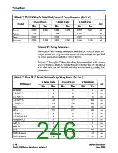
Table 6–73. Stratix GX I/O Standard Row Pin Input Delay Adders (Part 1 of 2)
-5 Speed Grade -6 Speed Grade
-7 Speed Grade
I/O Standard
Unit
Min
Max
Min
Max
Min
Max
LVCMOS
0
0
0
0
0
0
ps
ps
ps
ps
ps
ps
ps
ps
ps
ps
ps
ps
ps
ps
ps
ps
ps
ps
ps
ps
3.3-V LVTTL
2.5-V LVTTL
1.8-V LVTTL
1.5-V LVTTL
GTL
30
150
210
0
31
157
220
0
35
180
252
0
GTL+
220
0
231
0
265
0
3.3-V PCI
3.3-V PCI-X 1.0
Compact PCI
AGP 1×
0
0
0
0
0
0
0
0
0
AGP 2×
0
0
0
CTT
80
–30
–30
–70
–70
180
0
84
–32
–32
–74
–74
189
0
96
–37
–37
–86
–86
217
0
SSTL-3 class I
SSTL-3 class II
SSTL-2 class I
SSTL-2 class II
SSTL-18 class I
SSTL-18 class II
1.5-V HSTL class I
130
136
156
Altera Corporation
June 2006
6–45
Stratix GX Device Handbook, Volume 1

 ALTERA [ ALTERA CORPORATION ]