Timing Model
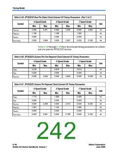
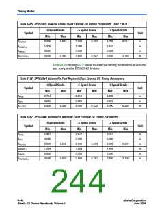
Table 6–71. EP1SGX40 Row Pin Global Clock External I/O Timing Parameters (Part 2 of 2)
-5 Speed Grade
-6 Speed Grade
-7 Speed Grade
Symbol
Unit
Min
Max
Min
Max
Min
Max
tOUTCO
tINSUPLL
tINHPLL
2.000
1.126
0.000
0.500
5.365
2.000
1.186
0.000
0.500
5.775
2.000
1.352
0.000
0.500
6.621
ns
ns
ns
ns
tOUTCOPLL
2.304
2.427
2.765
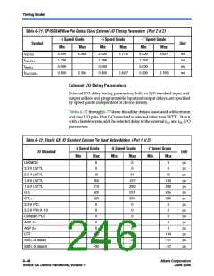
External I/O Delay Parameters
External I/O delay timing parameters, both for I/O standard input and
output adders and programmable input and output delays, are specified
by speed grade, independent of device density.
Tables 6–72 through 6–77 show the adder delays associated with column
and row I/O pins. If an I/O standard is selected other than LVTTL 24 mA
with a fast slew rate, add the selected delay to the external tCO and tSU I/O
parameters.
Table 6–72. Stratix GX I/O Standard Column Pin Input Delay Adders (Part 1 of 2)
-5 Speed Grade -6 Speed Grade -7 Speed Grade
I/O Standard
Unit
Min
Max
Min
Max
Min
Max
LVCMOS
0
0
0
0
0
0
ps
ps
ps
ps
ps
ps
ps
ps
ps
ps
ps
ps
ps
ps
ps
3.3-V LVTTL
2.5-V LVTTL
1.8-V LVTTL
1.5-V LVTTL
GTL
30
150
210
220
220
0
31
157
220
231
231
0
35
180
252
265
265
0
GTL+
3.3-V PCI
3.3-V PCI-X 1.0
Compact PCI
AGP 1×
0
0
0
0
0
0
0
0
0
AGP 2×
0
0
0
CTT
120
–30
–30
126
–32
–32
144
–37
–37
SSTL-3 class I
SSTL-3 class II
6–44
Altera Corporation
June 2006
Stratix GX Device Handbook, Volume 1

 ALTERA [ ALTERA CORPORATION ]