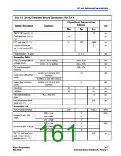
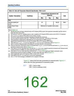
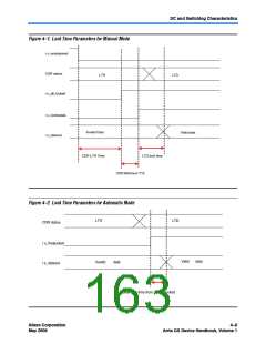
DC and Switching Characteristics
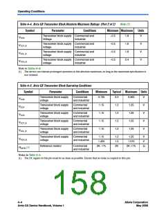
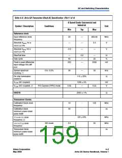
Table 4–6. Arria GX Transceiver Block AC Specification (Part 1 of 4)
-6 Speed Grade Commercial and
Industrial
Symbol / Description
Conditions
Unit
Min
Typ
Max
Reference clock
Input reference clock
frequency
50
—
—
—
622.08
3.3
MHz
V
Absolute VMAX for a
REFCLKPin
Absolute VMIN for a
-0.3
—
—
V
REFCLKPin
Rise/Fall time
Duty cycle
—
45
0.2
—
—
55
UI
%
Peak to peak differential
input voltage Vid (diff
p-p)
200
—
2000
mV
Spread spectrum
0 to -0.5%
30
—
33
kHz
clocking (1)
On-chip termination
resistors
115 20%
Ω
VICM (AC coupled)
1200 5%
—
mV
V
VICM (DC coupled) (2)
PCI Express (PIPE) mode
0.25
0.55
RREFB
2000 +/-1%
Ω
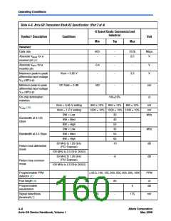
Transceiver Clocks
Calibration block clock
frequency
10
30
-
-
125
-
MHz
ns
Calibration block
minimum power-down
pulse width
125 10%
MHz
MHz
ns
fixedclkclock
frequency (3)
SDI mode
2.5
50
-
reconfigclock
frequency
Transceiver block
minimum power-down
pulse width
100
-
Altera Corporation
May 2008
4–5
Arria GX Device Handbook, Volume 1

 ALTERA [ ALTERA CORPORATION ]