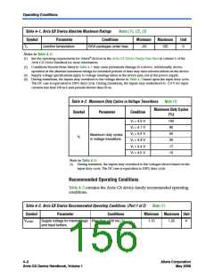
DC and Switching Characteristics
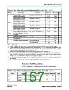
Table 4–3. Arria GX Device Recommended Operating Conditions (Part 2 of 2)
Note (1)
Symbol
Parameter
Conditions
Minimum Maximum Unit
Supply voltage for output
buffers, 3.3-V operation
Rise time ≤100 ms (3), (6)
3.135
(3.00)
3.465
(3.60)
V
V
V
V
V
V
Supply voltage for output
buffers, 2.5-V operation
Rise time ≤100 ms (3)
Rise time ≤100 ms (3)
Rise time ≤100 ms (3)
Rise time ≤100 ms (3)
2.375
2.625
Supply voltage for output
buffers, 1.8-V operation
1.71
1.89
VCCIO
Supply voltage for output
buffers, 1.5-V operation
1.425
1.15
1.575
1.25
Supply voltage for output
buffers, 1.2-V operation
Supply voltage forpre-driversas 100 μs ≤rise time ≤100 ms (4)
well as configuration and JTAG
3.135
3.465
VCCPD
I/O buffers.
VI
Input voltage (see Table 4–2)
Output voltage
(2), (5)
–0.5
0
4.0
VCCIO
85
V
V
C
C
VO
TJ
Operating junction temperature For commercial use
For industrial use
0
–40
100
Notes to Table 4–3:
(1) Supply voltage specifications apply to voltage readings taken at the device pins, not at the power supply.
(2) During transitions, the inputs may overshoot to the voltage shown in Table 4–2 based upon the input duty cycle.
The DC case is equivalent to 100% duty cycle. During transitions, the inputs may undershoot to –2.0 V for input
currents less than 100 mA and periods shorter than 20 ns.
(3) Maximum VCC rise time is 100 ms, and VCC must rise monotonically from ground to VCC
.
(4) VCCPD must ramp-up from 0 V to 3.3 V within 100 μs to 100 ms. If VCCPD is not ramped up within this specified
time, the Arria GX device will not configure successfully. If the system does not allow for a VCCPD ramp-up time of
100 ms or less, hold nCONFIGlow until all power supplies are reliable.
(5) All pins, including dedicated inputs, clock, I/O, and JTAG pins, may be driven before VCCINT, VCCPD, and VCCIO
are powered.
(6)
VCCIO maximum and minimum conditions for PCI and PCI-X are shown in parentheses.
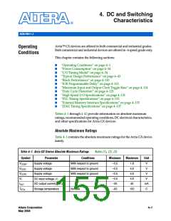
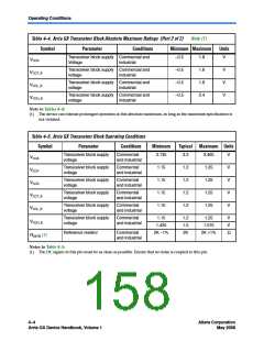
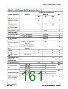
Transceiver Block Characteristics
Tables 4–4 through 4–6 contain transceiver block specifications.
Table 4–4. Arria GX Transceiver Block Absolute Maximum Ratings (Part 1 of 2)
Note (1)
Symbol Parameter Conditions Minimum Maximum
Units
Transceiver block supply Commercial and
voltage industrial
–0.5
–0.5
4.6
1.8
V
VCCA
VCCP
Transceiver block supply Commercial and
voltage industrial
V
Altera Corporation
May 2008
4–3
Arria GX Device Handbook, Volume 1

 ALTERA [ ALTERA CORPORATION ]