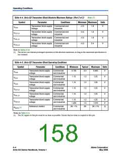
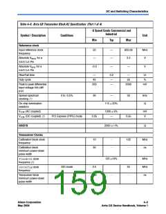
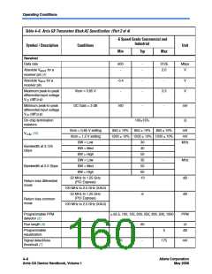
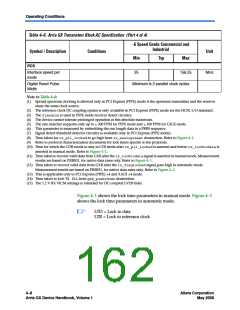
Operating Conditions
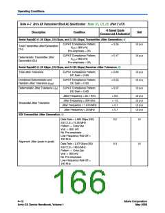
Table 4–6. Arria GX Transceiver Block AC Specification (Part 4 of 4)
-6 Speed Grade Commercial and
Industrial
Symbol / Description
Conditions
Unit
Min
Typ
Max
PCS
Interface speed per
mode
25
156.25
MHz
Digital Reset Pulse
Width
Minimum is 2 parallel clock cycles
Note to Table 4–6:
(1) Spread spectrum clocking is allowed only in PCI Express (PIPE) mode if the upstream transmitter and the receiver
share the same clock source.
(2) The reference clock DC coupling option is only available in PCI Express (PIPE) mode for the HCSL I/O standard.
(3) The fixedclkis used in PIPE mode receiver detect circuitry.
(4) The device cannot tolerate prolonged operation at this absolute maximum.
(5) The rate matcher supports only up to 300 PPM for PIPE mode and 100 PPM for GIGE mode.
(6) This parameter is measured by embedding the run length data in a PRBS sequence.
(7) Signal detect threshold detector circuitry is available only in PCI Express (PIPE mode).
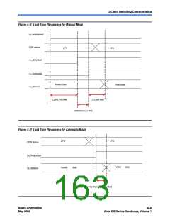
(8) Time taken for rx_pll_lockedto go high from rx_analogresetdeassertion. Refer to Figure 4–1.
(9) Refer to protocol characterization documents for lock times specific to the protocols.
(10) Time for which the CDR needs to stay in LTR mode after rx_pll_lockedis asserted and before rx_locktodatais
asserted in manual mode. Refer to Figure 4–1.
(11) Time taken to recover valid data from GXB after the rx_locktodatasignal is asserted in manual mode. Measurement
results are based on PRBS31, for native data rates only. Refer to Figure 4–1.
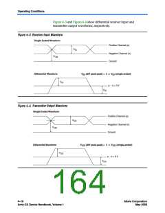
(12) Time taken to recover valid data from GXB after the rx_freqlockedsignal goes high in automatic mode.
Measurement results are based on PRBS31, for native data rates only. Refer to Figure 4–2.
(13) This is applicable only to PCI Express (PIPE) ×4 and XAUI ×4 mode.
(14) Time taken to lock TX PLLfrom gxb_powerdowndeassertion.
(15) The 1.2 V RX VICM settings is intended for DC-coupled LVDS links.
Figure 4–1 shows the lock time parameters in manual mode. Figure 4–2
shows the lock time parameters in automatic mode.
1
LTD = Lock to data
LTR = Lock to reference clock
4–8
Arria GX Device Handbook, Volume 1
Altera Corporation
May 2008

 ALTERA [ ALTERA CORPORATION ]