Selectable I/O Standards in Stratix II and Stratix II GX Devices
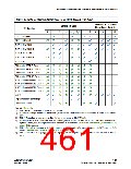
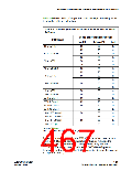
Table 4–4. Stratix II and Stratix II GX I/O Standards and Voltage Levels (Part 3 of 3) Note (1)
Stratix II and Stratix II GX
VCCIO (V)
VREF (V)
Input
VTT (V)
Input Operation
Top and Left and
Output Operation
I/O Standard
Top and
Bottom I/O
Banks
Left and
Right I/O
Banks(3)
Termination
Bottom I/O
Banks
Right I/O
Banks (3)
HyperTransport
technology
NA
2.5
NA
NA
2.5
NA
NA
NA
NA
Differential LVPECL 3.3/2.5/1.8/1.5
3.3
NA
(2)
Notes to Table 4–4:
(1) Any input pins with PCI-clamping diode will clamp the VCCIO to 3.3 V.
(2) LVDS and LVPECL output operation in the top and bottom banks is only supported in PLL banks 9-12. The VCCIO
level for differential output operation in the PLL banks is 3.3 V. The VCCIO level for output operation in the left and
right I/O banks is 2.5 V.
(3) The right I/O bank does not apply to the Stratix II GX. The right I/O Bank on Stratix II GX devices consists of
transceivers.
(4) 1.2-V HSTL is only supported in I/O banks 4,7, and 8.
f
Refer to the DC & Switching Characteristics chapter in volume 1 of the
Stratix II Device Handbook or the DC & Switching Characteristics chapter in
volume 1 of the Stratix II GX Device Handbook for detailed electrical
characteristics of each I/O standard.
Stratix II and Stratix II GX devices feature on-chip termination to provide
I/O impedance matching and termination capabilities. Apart from
maintaining signal integrity, this feature also minimizes the need for
external resistor networks, thereby saving board space and reducing
costs.
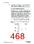
On-Chip
Termination
Stratix II and Stratix II GX devices support on-chip series (RS) and
parallel (RT) termination for single-ended I/O standards and on-chip
differential termination (RD) for differential I/O standards. This section
discusses the on-chip series termination support.
f
For more information on differential on-chip termination, Refer to the
High-Speed Differential I/O Interfaces with DPA in Stratix II & Stratix II GX
Devices chapter in volume 2 of the Stratix II Device Handbook or the
High-Speed Differential I/O Interfaces with DPA in Stratix II & Stratix II GX
Devices chapter in volume 2 of the Stratix II GX Device Handbook.
Altera Corporation
January 2008
4–27
Stratix II Device Handbook, Volume 2

 ALTERA [ ALTERA CORPORATION ]