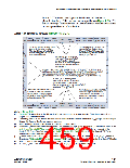
Selectable I/O Standards in Stratix II and Stratix II GX Devices
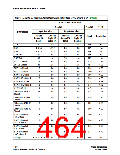
Table 4–3. I/O Standards Supported for Stratix II and Stratix II GX PLL Pins (Part 2 of 2)
Enhanced PLL (1)
Input
Fast PLL
Input
I/O Standard (2)
Output
INCLK
v
FBIN
v
EXTCLK
v
INCLK
1.8-V differential HSTL Class I
1.8-V differential HSTL Class II
1.5-V differential HSTL Class I
1.5-V differential HSTL Class II
LVDS
v
v
v
v
v
v
v
v
v
v
v
v
v
v
HyperTransport technology
Differential LVPECL
v
v
v
Note to Table 4–3:
(1) The enhanced PLL external clock output bank does not allow a mixture of both single-ended and differential I/O
standards.
(2) Altera does not support 1.2-V HSTL for PLL input pins on column I/O pins.
f
For more information, refer to the PLLs in Stratix II & Stratix II GX
Devices chapter in volume 2 of the Stratix II Device Handbook or the PLLs
in Stratix II & Straix II GX Devices chapter in volume 2 of the Stratix II GX
Device Handbook.
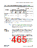
Voltage Levels
Stratix II device specify a range of allowed voltage levels for supported
I/O standards. Table 4–4 shows only typical values for input and output
VCCIO, VREF, as well as the board VTT.
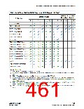
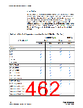
Table 4–4. Stratix II and Stratix II GX I/O Standards and Voltage Levels (Part 1 of 3) Note (1)
Stratix II and Stratix II GX
VCCIO (V)
VREF (V)
Input
VTT (V)
Input Operation
Top and Left and
Output Operation
I/O Standard
Top and
Bottom I/O
Banks
Left and
Right I/O
Banks(3)
Termination
Bottom I/O
Banks
Right I/O
Banks (3)
LVTTL
3.3/2.5
3.3/2.5
3.3/2.5
3.3/2.5
3.3
3.3
3.3
3.3
NA
NA
NA
NA
LVCMOS
Altera Corporation
January 2008
4–25
Stratix II Device Handbook, Volume 2

 ALTERA [ ALTERA CORPORATION ]