Selectable I/O Standards in Stratix II and Stratix II GX Devices
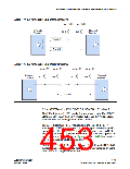
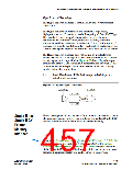
Figure 4–17. 1.5-V Differential HSTL Class II Termination
VTT = 0.75 V
VTT = 0.75 V
VTT = 0.75 V
VTT = 0.75 V
Differential
Transmitter
Differential
Receiver
50 Ω
50 Ω
50 Ω
50 Ω
Z
= 50 Ω
0
Z
= 50 Ω
0
LVDS
The LVDS standard is formulated under ANSI/TIA/EIA Standard,
ANSI/TIA/EIA-644: Electrical Characteristics of Low Voltage
Differential Signaling Interface Circuits.
The LVDS I/O standard is a differential high-speed, low-voltage swing,
low-power, general-purpose I/O interface standard. In Stratix II devices,
the LVDS I/O standard requires a 2.5-V VCCIO level for the side I/O pins
in banks 1, 2, 5, and 6. The top and bottom banks have different VCCIO
requirements for the LVDS I/O standard. The LVDS clock I/O pins in
banks 9 through 12 require a 3.3-V VCCIO level. Within these banks, the
PLL[5,6,11,12]_OUT[1,2]pins support output only LVDS
operations. The PLL[5,6,11,12]_FB/OUT2pins support LVDS input
or output operations but cannot be configured for bidirectional LVDS
operations. The LVDS clock input pins in banks 4, 5, 7, and 8 use VCCINT
and have no dependency on the VCCIO voltage level. This standard is used
in applications requiring high-bandwidth data transfer, backplane
drivers, and clock distribution. The ANSI/TIA/EIA-644 standard
specifies LVDS transmitters and receivers capable of operating at
recommended maximum data signaling rates of 655 megabit per second
(Mbps). However, devices can operate at slower speeds if needed, and
there is a theoretical maximum of 1.923 Gbps. Stratix II and Stratix II GX
devices are capable of running at a maximum data rate of 1 Gbps and still
meet the ANSI/TIA/EIA-644 standard.
Because of the low-voltage swing of the LVDS I/O standard, the
electromagnetic interference (EMI) effects are much smaller than
complementary metal-oxide semiconductor (CMOS),
transistor-to-transistor logic (TTL), and positive (or psuedo) emitter
coupled logic (PECL). This low EMI makes LVDS ideal for applications
Altera Corporation
January 2008
4–17
Stratix II Device Handbook, Volume 2

 ALTERA [ ALTERA CORPORATION ]