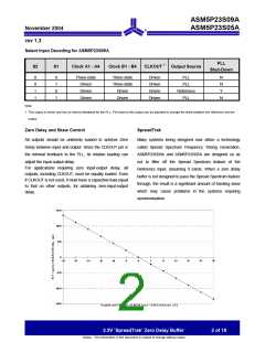
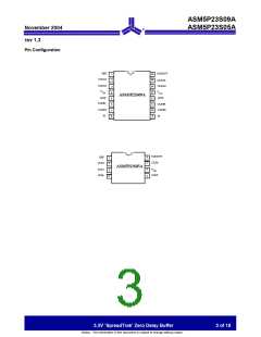
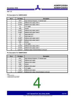
ASM5P23S09A
ASM5P23S05A
November 2004
rev 1.3
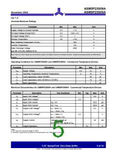
Switching Characteristics for ASM5P23S05A-1 and ASM5P23S09A-1 Commercial Temperature Devices7
Parameter
Description
Test Conditions
Min
Typ
Max
Unit
1/t1
Output Frequency
30-pF load
10-pF load
15
15
100
133
MHz
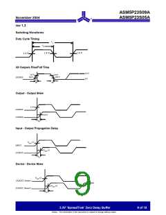
Duty Cycle 8 = (t2 / t1) * 100 Measured at 1.4V, FOUT = 66.67 MHz
40.0
50.0
60.0
2.50
2.50
250
%
t3
t4
t5
t6
Output Rise Time 8
Output Fall Time 8
Output-to-output skew 8
Measured between 0.8V and 2.0V
Measured between 2.0V and 0.8V
All outputs equally loaded
nS
nS
pS
pS
Delay, REF Rising Edge to Measured at VDD /2
CLKOUT Rising Edge 8
0
0
±350
t7
Device-to-Device Skew 8
Measured at VDD/2 on the CLKOUT pins of
700
pS
the device
tJ
Cycle-to-cycle jitter 8
PLL Lock Time 8
Measured at 66.67 MHz, loaded outputs
Stable power supply, valid clock presented
on REF pin
200
1.0
pS
tLOCK
mS
Notes:
7. All parameters specified with loaded outputs.
8. Parameter is guaranteed by design and characterization. Not 100% tested in production
Operating Conditions for ASM5I23S05A and ASM5I23S09A Industrial Temperature Devices
Parameter
Description
Min
Max
Unit
VDD
TA
Supply Voltage
3.0
-40
3.6
85
30
15
7
V
Operating Temperature (Ambient Temperature)
Load Capacitance, below 100 MHz
Load Capacitance, from 100 MHz to 133 MHz
Input Capacitance
°C
pF
pF
pF
CL
CL
CIN
3.3V ‘SpreadTrak’ Zero Delay Buffer
6 of 18
Notice: The information in this document is subject to change without notice.

 ALSC [ ALLIANCE SEMICONDUCTOR CORPORATION ]