PDF
最近搜索
热门搜索
发布采购

| 型号: | ASM5P23S05AF-1-08-TR |
| PDF下载: | 下载PDF文件 查看货源 |
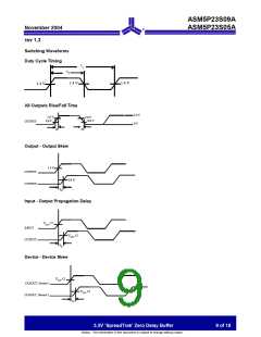
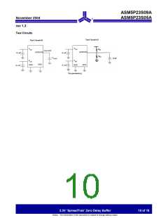
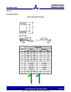
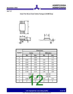
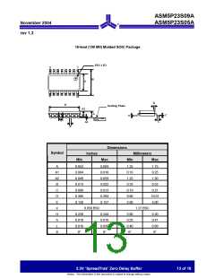
| 内容描述: | 3.3V SpreadTrak零延迟缓冲器 [3.3V SpreadTrak Zero Delay Buffer] |
| 分类和应用: | 时钟驱动器逻辑集成电路光电二极管 |
| 文件页数/大小: | 18 页 / 382 K |
| 品牌: |  ALSC [ ALLIANCE SEMICONDUCTOR CORPORATION ] ALSC [ ALLIANCE SEMICONDUCTOR CORPORATION ] |
专业IC领域供求交易平台:提供全面的IC Datasheet资料和资讯,Datasheet 1000万数据,IC品牌1000多家。