ASM5P23S09A
ASM5P23S05A
November 2004
rev 1.3
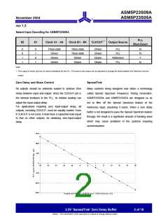
Select Input Decoding for ASM5P23S09A
PLL
S2
S1
Clock A1 - A4
Clock B1 - B4
CLKOUT 1 Output Source
Shut-Down
0
0
1
1
0
1
0
1
Three-state
Driven
Three-state
Three-state
Driven
Driven
Driven
Driven
Driven
PLL
PLL
N
N
Y
N
Driven
Reference
PLL
Driven
Driven
Note:
1. This output is driven and has an internal feedback for the PLL. The load on this output can be adjusted to change the skew between the reference and the
output.
Zero Delay and Skew Control
SpreadTrak
All outputs should be uniformly loaded to achieve Zero
Delay between input and output. Since the CLKOUT pin is
the internal feedback to the PLL, its relative loading can
Many systems being designed now utilize a technology
called Spread Spectrum Frequency Timing Generation.
ASM5P23S09A and ASM5P23S05A are designed so as
not to filter off the Spread Spectrum feature of the
Reference input, assuming it exists. When a zero delay
buffer is not designed to pass the Spread Spectrum feature
through, the result is a significant amount of tracking skew
which may cause problems in the systems requiring
synchronization.
adjust the input-output delay.
For applications requiring zero input-output delay, all
outputs, including CLKOUT, must be equally loaded. Even
if CLKOUT is not used, it must have a capacitive load equal
to that on other outputs, for obtaining zero-input-output
delay.
3.3V ‘SpreadTrak’ Zero Delay Buffer
2 of 18
Notice: The information in this document is subject to change without notice.

 ALSC [ ALLIANCE SEMICONDUCTOR CORPORATION ]