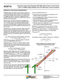
Automotive Grade, Fully Integrated, Hall Effect-Based Linear Current Sensor
with 2.1 kVRMS Voltage Isolation and a Low-Resistance Current Conductor
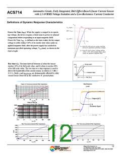
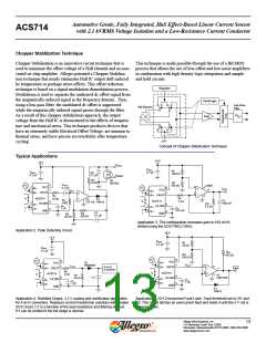
ACS714
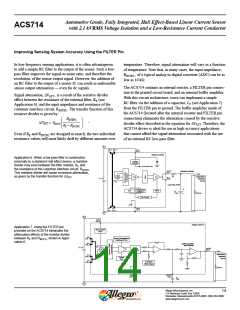
Improving Sensing System Accuracy Using the FILTER Pin
In low-frequency sensing applications, it is often advantageous
to add a simple RC filter to the output of the sensor. Such a low-
pass filter improves the signal-to-noise ratio, and therefore the
resolution, of the sensor output signal. However, the addition of
an RC filter to the output of a sensor IC can result in undesirable
sensor output attenuation — even for dc signals.
temperature. Therefore, signal attenuation will vary as a function
of temperature. Note that, in many cases, the input impedance,
RINTFC , of a typical analog-to-digital converter (ADC) can be as
low as 10 kꢀ.
The ACS714 contains an internal resistor, a FILTER pin connec-
tion to the printed circuit board, and an internal buffer amplifier.
With this circuit architecture, users can implement a simple
RC filter via the addition of a capacitor, CF (see Application 7)
from the FILTER pin to ground. The buffer amplifier inside of
the ACS714 (located after the internal resistor and FILTER pin
connection) eliminates the attenuation caused by the resistive
divider effect described in the equation for ∆VATT. Therefore, the
ACS714 device is ideal for use in high-accuracy applications
that cannot afford the signal attenuation associated with the use
of an external RC low-pass filter.
Signal attenuation, ∆VATT , is a result of the resistive divider
effect between the resistance of the external filter, RF (see
Application 6), and the input impedance and resistance of the
customer interface circuit, RINTFC. The transfer function of this
resistive divider is given by:
RINTFC
⎛
⎞
.
∆VATT
V
⎜
⎜
=
IOUT
⎟
RF + RINTFC
⎝
⎠
Even if RF and RINTFC are designed to match, the two individual
resistance values will most likely drift by different amounts over
+5 V
Pin 3 Pin 4
VCC
Pin 8
IP–
IP–
Allegro ACS706
Application 6. When a low pass filter is constructed
externally to a standard Hall effect device, a resistive
divider may exist between the filter resistor, RF, and
the resistance of the customer interface circuit, RINTFC
This resistive divider will cause excessive attenuation,
Voltage
Regulator
To all subcircuits
.
VIOUT
Pin 7
Resistive Divider
Input
RF
Amp
Out
Application
Interface
Circuit
as given by the transfer function for ∆VATT
.
N.C.
Pin 6
0.1 MF
Low Pass Filter
Temperature
Coefficient
Gain
Offset
CF
1 nF
RINTFC
Trim Control
GND
Pin 5
IP+
Pin 1 Pin 2
IP+
+5 V
VCC
Pin 8
Allegro ACS714
Application 7. Using the FILTER pin
provided on the ACS714 eliminates the
attenuation effects of the resistor divider
between RF and RINTFC, shown in Appli-
cation 6.
Hall Current
Drive
IP+
Sense Temperature
Coefficient Trim
Pin 1
IP+
Pin 2
Buffer Amplifier
and Resistor
Signal
Recovery
VIOUT
Pin 7
Input
Application
Interface
Circuit
IP–
Pin 3
Sense
Trim
IP–
Pin 4
0 Ampere
Offset Adjust
RINTFC
GND
Pin 5
FILTER
Pin 6
CF
1 nF
Allegro MicroSystems, Inc.
115 Northeast Cutoff, Box 15036
14
Worcester, Massachusetts 01615-0036 (508) 853-5000
www.allegromicro.com

 ALLEGRO [ ALLEGRO MICROSYSTEMS ]