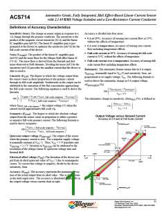
Automotive Grade, Fully Integrated, Hall Effect-Based Linear Current Sensor
with 2.1 kVRMS Voltage Isolation and a Low-Resistance Current Conductor
ACS714
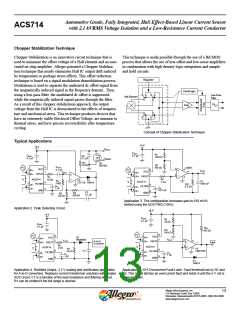
Chopper Stabilization Technique
Chopper Stabilization is an innovative circuit technique that is
This technique is made possible through the use of a BiCMOS
used to minimize the offset voltage of a Hall element and an asso- process that allows the use of low-offset and low-noise amplifiers
ciated on-chip amplifier. Allegro patented a Chopper Stabiliza-
tion technique that nearly eliminates Hall IC output drift induced
by temperature or package stress effects. This offset reduction
technique is based on a signal modulation-demodulation process.
Modulation is used to separate the undesired dc offset signal from
the magnetically induced signal in the frequency domain. Then,
using a low-pass filter, the modulated dc offset is suppressed
while the magnetically induced signal passes through the filter.
As a result of this chopper stabilization approach, the output
voltage from the Hall IC is desensitized to the effects of tempera-
ture and mechanical stress. This technique produces devices that
have an extremely stable Electrical Offset Voltage, are immune to
thermal stress, and have precise recoverability after temperature
cycling.
in combination with high-density logic integration and sample
and hold circuits.
Regulator
Clock/Logic
Low-Pass
Filter
Hall Element
Amp
Concept of Chopper Stabilization Technique
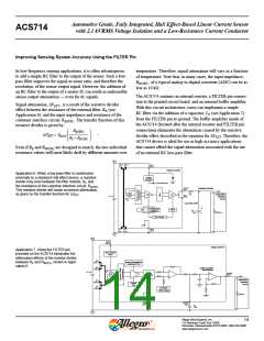
Typical Applications
+5 V
+5 V
VPEAK
CBYP
0.1 μF
R1
CBYP
0.1 μF
C2
100 kΩ
0.1 μF
VRESET
R4
Q1
2N7002
10 kΩ
R2
COUT
8
7
100 kΩ
LM321
4
1
3
1
+
–
VCC
5
2
0.1 μF
8
7
IP+
VOUT
1
2
VCC
VOUT
+
–
IP+
IP+
2
VIOUT
IP+
VIOUT
RF
10 kΩ
IP
RF
1 kΩ
ACS714
U1
D1
R1
1 MΩ
CF
C1
IP
ACS714
6
5
LT1178 1N914
3
4
1000 pF
FILTER
R3
6
5
IP–
IP–
3
4
FILTER
3.3 kΩ
IP–
IP–
CF
0.01 μF
1 nF
GND
C1
R3
GND
R2
33 kΩ
0.1 μF
330 kΩ
Application 3. This configuration increases gain to 610 mV/A
(tested using the ACS714ELC-05A).
Application 2. Peak Detecting Circuit
+5 V
+5 V
CBYP
0.1 μF
R1
33 kΩ
CBYP
0.1 μF
RPU
R2
100 kΩ
100 kΩ
8
7
8
1
2
VCC
1
D1
VCC
IP+
IP+
IP+
VOUT
1N4448W
4
3
VOUT
7
5
2
2
A-to-D
Converter
VIOUT
–
+
Fault
VIOUT
IP+
1
RF
IP
ACS714
ACS714
IP
2 kΩ
U1
R1
10 kΩ
CF
1 nF
6
5
3
4
C1
6
5
LMV7235
FILTER
3
4
IP–
IP–
FILTER
GND
CF
IP–
IP–
1 nF
GND
D1
1N914
Application 4. Rectified Output. 3.3 V scaling and rectification application
for A-to-D converters. Replaces current transformer solutions with simpler
ACS circuit. C1 is a function of the load resistance and filtering desired.
R1 can be omitted if the full range is desired.
Application 5. 10 A Overcurrent Fault Latch. Fault threshold set by R1 and
R2. This circuit latches an overcurrent fault and holds it until the 5 V rail is
powered down.
Allegro MicroSystems, Inc.
115 Northeast Cutoff, Box 15036
13
Worcester, Massachusetts 01615-0036 (508) 853-5000
www.allegromicro.com

 ALLEGRO [ ALLEGRO MICROSYSTEMS ]