[AK8975/C]
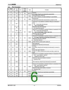
4.3. Pin Function
Pin No.
Power
supply
system
Pin
I/O
Type
Function
name
75
75C
Test pin.
1
2
A1
A2
TST1
CSB
O
I
VDD
VID
ANALOG
CMOS
Hi-Z output. Keep this pin electrically nonconnected.
Chip select pin for 4-wire SPI.
“L” active. Connect to VID when selecting I2C bus interface.
Reserved pin.
3
A4
RSV
SCL
I
VID
CMOS
Keep this pin electrically nonconnected or connect to VSS.
When the I2C bus interface is selected (CSB pin is connected to
VID)
SCL: Control data clock input pin
4
A3
I
VID
CMOS
Input: Schmidt trigger
When the 4-wire SPI is selected
SK
SDA
SI
SK: Serial clock input pin
When the I2C bus interface is selected (CSB pin is connected to VID)
SDA: Control data input/output pin
Input: Schmidt trigger, Output: Open drain
When the 4-wire SPI is selected
I/O
I
5
6
D4
B4
VID
CMOS
SI: Serial data input pin
When the I2C bus interface is selected (CSB pin is connected to VID)
Hi-Z output. Keep this pin electrically nonconnected.
When the 4-wire SPI is selected
SO
O
-
VID
-
CMOS
Power
Serial data output pin
7
8
C4
-
VID
Digital interface positive power supply pin.
Non-contact pin.
NC1
Keep this pin electrically nonconnected.
Test pin.
9
B3
C3
TST6
O
O
VID
VID
CMOS
CMOS
Vss output. Keep this pin electrically nonconnected or connect to
VSS..
Data ready signal output pin.
10
DRDY
Active “H”. Informs measurement ended and data is ready to be
read.
When the I2C bus interface is selected (CSB pin is connected to VID)
CAD1: Slave address 1 input pin
Connect to VSS or VDD.
11
12
D2
CAD1
NC2
I
VDD
CMOS
When the 4-wire serial interface is selected
Connect to VSS.
-
Non-contact pin. Keep this pin electrically nonconnected.
When the I2C bus interface is selected (CSB pin is connected to VID)
CAD0: Slave address 0 input pin
Connect to VSS or VDD.
13
14
D1
C2
CAD0
TST2
I
VDD
VDD
CMOS
When the 4-wire serial interface is selected
Connect to VSS.
Test pin.
O
ANALOG
Hi-Z output. Keep this pin electrically nonconnected.
15
16
C1
B1
VSS
VDD
-
-
-
-
Power
Power
Ground pin.
Analog Power supply pin.
MS1187-E-02
- 6 -
2010/05

 AKM [ ASAHI KASEI MICROSYSTEMS ]