[AK8975/C]
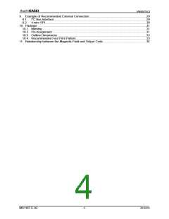
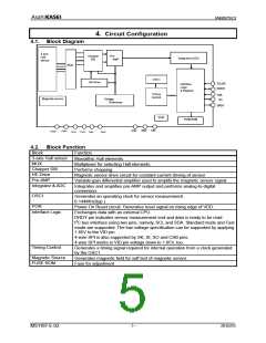
4. Circuit Configuration
4.1. Block Diagram
3-axis
Hall
sensor
Chopper
SW
Pre-
AMP
Integrator&ADC
MUX
OSC1
HE-Drive
SCL/SK
SDA/SI
Interface,
Logic
& Register
Timing
Control
CSB
SO
Magnetic source
Voltage
Reference
DRDY
POR
FUSE ROM
VDD
VID
CAD1
VSS
CAD0
TST1
TST2
RSV
TST6
4.2. Block Function
Block
Function
3-axis Hall sensor
MUX
Chopper SW
HE-Drive
Monolithic Hall elements.
Multiplexer for selecting Hall elements.
Performs chopping.
Magnetic sensor drive circuit for constant-current driving of sensor
Pre-AMP
Variable-gain differential amplifier used to amplify the magnetic sensor signal.
Integrator & ADC
Integrates and amplifies pre-AMP output and performs analog-to-digital
conversion.
OSC1
Generates an operating clock for sensor measurement.
6.144MHz(typ.)
POR
Power On Reset circuit. Generates reset signal on rising edge of VDD.
Interface Logic
Exchanges data with an external CPU.
DRDY pin indicates sensor measurement end and data is ready to be read.
I2C bus interface using two pins, namely, SCL and SDA. Standard mode and Fast
mode are supported. The low-voltage specification can be supported by applying
1.65V to the VID pin.
4-wire SPI is also supported by SK, SI, SO and CSB pins.
4-wire SPI works in VID pin voltage down to 1.65V, too.
Timing Control
Generates a timing signal required for internal operation from a clock generated
by the OSC1.
Magnetic Source
FUSE ROM
Generates magnetic field for self test of magnetic sensor.
Fuse for adjustment
MS1187-E-02
- 5 -
2010/05

 AKM [ ASAHI KASEI MICROSYSTEMS ]