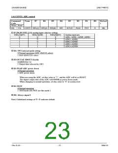
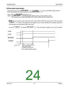
[ASAHI KASEI]
[AK7740ET]
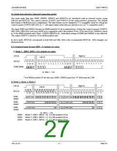
(6) Audio data interface (internal connection mode)
The serial audio data pins SDIN, SDINA, SDOUT and SDOUTA are interfaced with an external system, using
LRCLK and BITCLK. The control registers (CONT2 and CONT3) set the audio interface parameters. The default
2
data format is MSB-first two's complement. The data format can be changed to I S compatible mode by setting the
2
control register CONT0:DIF (D5) to “1” (all input/output audio data pin interfaces are in I S compatible mode.)
The input SDIN and SDINA formats are MSB justified 24-bit at initialization. Setting the control registers CONT0:
DIF1 (D4), DIF0 (D3) will cause SDIN to be compatible with LSB justified 24-bit, 20-bit and 16-bit. (SDINA is fixed
to 24-bit MSB justified only) (Note: CONT0 DIF(D5)=0). Individual setting of SDIN and SDINA is not allowed.
The output SDOUT is fixed at 24-bit MSB justified only.
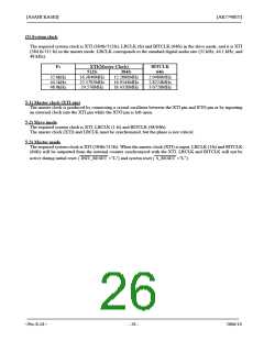
In slave mode, BITCLK corresponds to both 64fs and 48fs. 64fs is the recommended BITCLK. 64fs examples are
illustrated here:
6-1) Standard input format (DIF = 0: default set value)
a) Mode 1 (DIF1, DIF0 = 0,0: default set value)
LRCLK
Right ch
Left ch
BITCLK
10 9
8
L
7
6
5
4
3
2
1
0
31 30 29
M 22 21
10 9
8
L
7
6
5
4
3
2
1 0
31 30 29
M 22 21
SDIN,SDINA
2
1
2 1
M : MSB, L : LSB
* For MSB-justified 20-bit data into SDIN, SDINA input four "0" following the LSB.
b) Mode 2, Mode 3, Mode 4
LRCLK
Right ch
Left ch
BITCLK
1
0
L
1
0
31 30
23 22 21 20 19 18 17 16 15
M 22 21 20 19 18 17 16 15
23 22 21 20 19 18 17 16 15
M 22 21 20 19 18 17 16 15
31 30
SDIN
mode2
Don't Care
Don't Care
Don't Care
1
L
Don't Care
1
SDIN
mode3
1
1
L
L
M 18 17 16 15
M
M 18 17 16 15
M
1
1
L
L
Don't Care
Don't Care
SDIN
mode4
M : MSB, L : LSB
SDIN
SDIN
SDIN
Mode 2: (DIF1, DIF0) = (0, 1) LSB justified 24-bit
Mode 3: (DIF1, DIF0) = (1, 0) LSB justified 20-bit
Mode 4: (DIF1, DIF0) = (1, 1) LSB justified 16-bit
<Pre-E-01>
- 27 -
2006/10

 AKM [ ASAHI KASEI MICROSYSTEMS ]