ASAHI KASEI
[AK5385B]
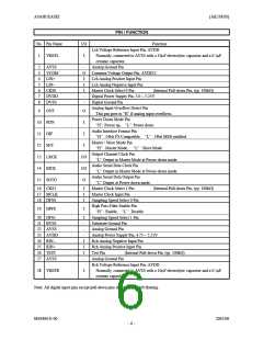
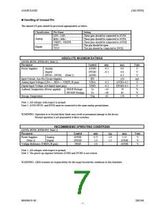
Handling of Unused Pin
The unused I/O pins should be processed appropriately as below.
Classification
Analog
Pin Name
Setting
These pins should be connected to AVSS.
These pins should be connected to AVSS.
These pins should be connected to AVDD.
This pin should be open.
LIN+, LIN−
RIN+, RIN−
VREFL, VREFR
OVF
Digital
TEST
This pin should be connected to DVSS.
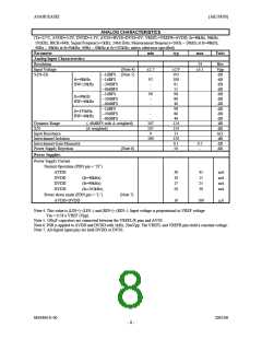
ABSOLUTE MAXIMUM RATINGS
Symbol
(AVSS, BVSS, DVSS=0V; Note 1)
Parameter
min
−0.3
−0.3
-
max
Units
V
V
Power Supplies:
Analog
AVDD
DVDD
∆GND
IIN
6.0
6.0
0.3
Digital
|BVSS – DVSS|
(Note 2)
V
Input Current, Any Pin Except Supplies
-
±10
mA
V
Analog Input Voltage (LIN+/–, RIN+/–, VREFL/R pins)
Digital Input Voltage (All digital input pins)
VINA
VIND
Ta
−0.3
−0.3
−10
−40
−65
AVDD+0.3
DVDD+0.3
70
V
Ambient Temperature (Power applied)
28SOP Package
°C
°C
°C
28VSOP Package
Ta
85
150
Storage Temperature
Tstg
Note 1. All voltages with respect to ground.
Note 2. AVSS BVSS, and DVSS must be connected to the same analog ground plane.
WARNING: Operation at or beyond these limits may result in permanent damage to the device.
Normal operation is not guaranteed at these extremes.
RECOMMENDED OPERATING CONDITIONS
(AVSS, BVSS, DVSS=0V; Note 1)
Parameter
Power Supplies
(Note 3)
Symbol
AVDD
DVDD
VREF
min
4.75
3.0
typ
5.0
3.3
-
max
5.25
AVDD
AVDD
Units
V
V
Analog
Digital
Voltage Reference (VREFL/R pins)
3.0
V
Note 1. All voltages with respect to ground.
Note 3. The power up sequence between AVDD and DVDD is not critical.
WARNING: AKM assumes no responsibility for the usage beyond the conditions in this datasheet.
MS0406-E-00
2005/08
- 7 -

 AKM [ ASAHI KASEI MICROSYSTEMS ]