ASAHI KASEI
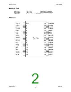
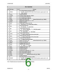
No. Pin Name
[AK5385B]
PIN / FUNCTION
I/O
I
Function
Lch Voltage Reference Input Pin, AVDD
1
VREFL
Normally, connected to AVSS with a 10µF electrolytic capacitor and a 0.1µF
ceramic capacitor.
2
3
4
5
6
7
8
AVSS
VCOM
LIN+
-
O
I
Analog Ground Pin
Common Voltage Output Pin, AVDD/2
Lch Analog Positive Input Pin
LIN−
I
Lch Analog Negative Input Pin
CKS0
DVDD
DVSS
I
Master Clock Select 0 Pin
(Internal Pull-down Pin, typ. 100kΩ)
-
Digital Power Supply Pin, 3.0 ∼ 5.25V
Digital Ground Pin
-
Analog Input Overflow Detect Pin
9
OVF
O
I
This pin goes to “H” if analog input overflows.
Power Down Mode Pin
10 PDN
11 DIF
“H”: Power up, “L”: Power down
Audio Interface Format Pin
I
“H” : 24bit I2S Compatible, “L” : 24bit MSB justified
Master / Slave Mode Pin
12 M/S
I
“H” : Master Mode, “L” : Slave Mode
Output Channel Clock Pin
13 LRCK
14 BICK
15 SDTO
I/O
I/O
O
“L” Output in Master Mode at Power-down mode.
Audio Serial Data Clock Pin
“L” Output in Master Mode at Power-down mode.
Audio Serial Data Output Pin
“L” Output at Power-down mode.
16 CKS1
17 MCLK
18 DFS0
I
I
I
Master Clock Select 1 Pin
Master Clock Input Pin
(Internal Pull-down Pin, typ. 100kΩ)
Sampling Speed Select 0 Pin
High Pass Filter Enable Pin
“H” : Enable, “L” : Disable
Sampling Speed Select 1 Pin
Substrate Ground Pin
19 HPFE
I
20 DFS1
21 BVSS
22 AVSS
23 AVDD
24 RIN−
25 RIN+
26 TEST
27 AVSS
I
-
-
-
I
I
I
-
Analog Ground Pin
Analog Power Supply Pin, 4.75 ∼ 5.25V
Rch Analog Negative Input Pin
Rch Analog Positive Input Pin
Test Pin
(Internal Pull-down Pin, typ. 100kΩ)
Analog Ground Pin
Rch Voltage Reference Input Pin, AVDD
Normally, connected to AVSS with a 10µF electrolytic capacitor and a 0.1µF
ceramic capacitor.
28 VREFR
I
Note: All digital input pins except pull-down pins should not be left floating.
MS0406-E-00
2005/08
- 6 -

 AKM [ ASAHI KASEI MICROSYSTEMS ]