ASAHI KASEI
[AK5385B]
SYSTEM DESIGN
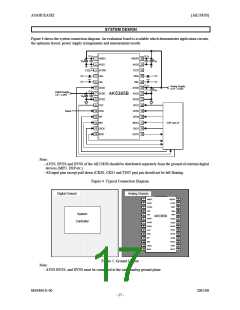
Figure 4 shows the system connection diagram. An evaluation board is available which demonstrates application circuits,
the optimum layout, power supply arrangements and measurement results.
0.1µ
0.1µ
1
2
3
4
5
6
7
8
9
VREFL
AVSS
VCOM
LIN+
VREFR 28
AVSS 27
TEST 26
RIN+ 25
RIN- 24
10µ
10µ
0.22µ
LIN-
0.1µ
Analog Supply
4.75 ~ 5.25V
CKS0
DVDD
DVSS
OVF
AVDD 23
AVSS 22
BVSS 21
DFS1 20
HPFE 19
DFS0 18
MCLK 17
CKS1 16
SDTO 15
10µ
0.1µ
Digital Supply
3.0 ~ 5.25V
AK5385B
10µ
Reset
10 PDN
11 DIF
12 M/S
13 LRCK
14 BICK
DSP and uP
Note:
- AVSS, BVSS and DVSS of the AK5385B should be distributed separately from the ground of external digital
devices (MPU, DSP etc.).
- All input pins except pull-down (CKS0, CKS1 and TEST pin) pin should not be left floating.
Figure 4. Typical Connection Diagram
Digital Ground
Analog Ground
1
2
3
4
5
6
7
8
9
28
VREFL
AVSS
VREFR
AVSS 27
TEST 26
VCOM
25
LIN+
RIN+
System
Controller
LIN-
RIN- 24
AK5385B
CKS0
DVDD
DVSS
OVF
23
22
21
AVDD
AVSS
BVSS
DFS1 20
HPFE 19
10 PDN
11 DIF
18
17
DFS0
MCLK
12 M/S
13 LRCK
CKS1 16
SDTO 15
BICK
14
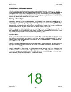
Figure 5. Ground Layout
Note:
- AVSS BVSS, and DVSS must be connected to the same analog ground plane.
MS0406-E-00
2005/08
- 17 -

 AKM [ ASAHI KASEI MICROSYSTEMS ]