ASAHI KASEI
[AK5385B]
Digital High Pass Filter
The ADC has a digital high pass filter for DC offset cancellation. The cut-off frequency of the HPF is 1.0Hz
(@fs=48kHz) and scales with sampling rate (fs).
HPF is controlled by HPFE pin. If HPF setting (ON/OFF) is changed at operating, click noise occurs by changing DC
offset. It is recommended that HPF setting is changed at PDN pin = “L”.
Overflow Detection
The AK5385B has overflow detect function for analog input. OVF pin goes to “H” if Lch or Rch overflows (more than
−0.3dBFS). OVF output for overflowed analog input has the same group delay as ADC (GD=43.2/fs=0.9ms@fs=48kHz).
OVF is “L” for 516/fs (=10.75ms@fs=48kHz) after PDN pin = “↑”, and then overflow detection is enabled.
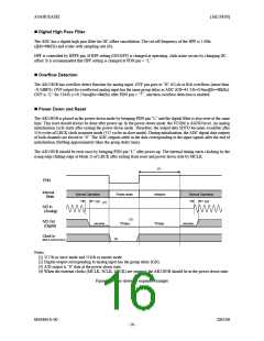
Power Down and Reset
The AK5385B is placed in the power-down mode by bringing PDN pin “L” and the digital filter is also reset at the same
time. This reset should always be done after power-up. In the power-down mode, the VCOM is AGND level. An analog
initialization cycle starts after exiting the power-down mode. Therefore, the output data SDTO becomes available after
516 cycles of LRCK clock in master mode (517 cycles in slave mode). During initialization, the ADC digital data outputs
of both channels are forced to “0”. The ADC outputs settle in the data corresponding to the input signals after the end of
initialization (Settling approximately takes the group delay time).
The AK5385B should be reset once by bringing PDN pin “L” after power-up. The internal timing starts clocking by the
rising edge (falling edge at Mode 1) of LRCK after exiting from reset and power down state by MCLK.
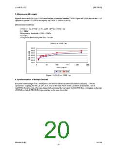
(1)
PDN
Internal
State
Normal Operation
GD
Power-down
Initialize
“0”data
Normal Operation
GD
(2)
A/D In
(Analog)
(3)
“0”data
A/D Out
(Digital)
Idle Noise
Idle Noise
Clock In
MCLK,LRCK,SCLK
(4)
Notes:
(1) 517/fs in slave mode and 516/fs in master mode.
(2) Digital output corresponding to analog input has the group delay (GD).
(3) A/D output is “0” data at the power-down state.
(4) When the external clocks (MCLK, SCLK, LRCK) are stopped, the AK5385B should be in the power-down state.
Figure 3. Power-down/up sequence example
MS0406-E-00
2005/08
- 16 -

 AKM [ ASAHI KASEI MICROSYSTEMS ]