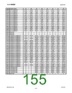
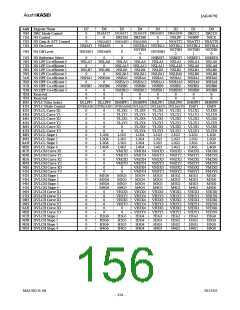
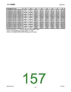
[AK4679]
D0
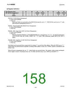
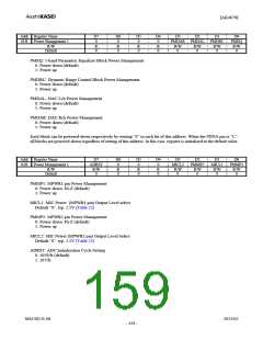
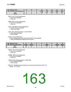
Addr Register Name
01H Power Management 1
D7
0
R
0
D6
0
R
0
D5
0
R
0
D4
0
R
0
D3
D2
D1
PMDAR PMDAL PMDRC
PMEQ
R/W
0
R/W
Default
R/W
0
R/W
0
R/W
0
PMEQ: 5-band Parametric Equalizer Block Power Management
0: Power down (default)
1: Power up
PMDRC: Dynamic Range Control Block Power Management
0: Power down (default)
1: Power up
PMDAL: DAC Lch Power Management
0: Power down (default)
1: Power up
PMDAR: DAC Rch Power Management
0: Power down (default)
1: Power up
Each block can be powered-down respectively by writing “0” in each bit of this address. When the PDNA pin is “L”,
all blocks are powered-down regardless of setting of this address. In this case, register is initialized to the default value.
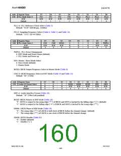
Addr Register Name
02H Power Management 1
D7
ADRST
R/W
0
D6
0
R
0
D5
0
R
0
D4
0
R
0
D3
MICL2
R/W
0
D2
PMMP2
R/W
0
D1
MICL1
R/W
0
D0
PMMP1
R/W
0
R/W
Default
PMMP1: MPWR1 pin Power Management
0: Power down: Hi-Z (default)
1: Power up
MICL1: MIC Power (MPWR1 pin) Output Level select
Default “0”, typ. 2.5V (Table 22)
PMMP2: MPWR2 pin Power Management
0: Power down: Hi-Z (default)
1: Power up
MICL2: MIC Power (MPWR2 pin) Output Level Select
Default “0”, typ. 2.5V (Table 22)
ADRST: ADC Initialization Cycle Setting
0: 1059/fs (default)
1: 267/fs
MS1402-E-06
2013/02
- 159 -

 AKM [ ASAHI KASEI MICROSYSTEMS ]