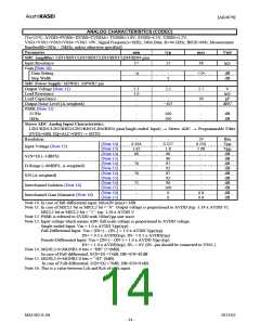
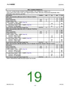
[AK4679]
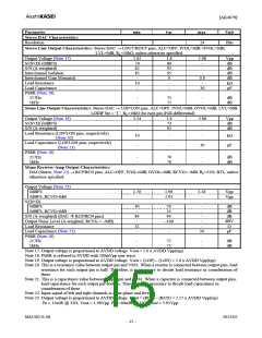
Parameter
min
typ
max
Unit
Stereo DAC Characteristics:
Resolution
-
-
24
Bits
Stereo Line Output Characteristics: Stereo DAC → LOUT/ROUT pins, ALC=OFF, IVOL=0dB, OVOL=0dB,
LVL=0dB, RL=10kΩ; unless otherwise specified.
Output Voltage (Note 17)
S/(N+D) (0dBFS)
S/N (A-weighted)
Interchannel Isolation
Interchannel Gain Mismatch
Load Resistance
Load Capacitance
PSRR (Note 18)
217Hz
1.62
70
82
85
-
1.8
80
92
95
0
1.98
-
-
-
0.8
-
Vpp
dB
dB
dB
dB
kΩ
pF
10
-
-
-
30
-
-
75
75
-
-
dB
dB
1kHz
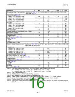
Mono Line Output Characteristics: Stereo DAC → LOP/LON pins, ALC=OFF, IVOL=0dB, OVOL=0dB, LVL=0dB,
LODIF bit = “1”, RL=10kΩ for each pin (Full-differential)
Output Voltage (Note 19)
S/(N+D) (0dBFS)
S/N (A-weighted)
3.24
-
-
3.6
73
95
3.96
-
-
Vpp
dB
dB
Load Resistance (LOP/LON pins, respectively)
10
-
-
-
-
kΩ
(Note 20)
Load Capacitance (LOP/LON pins, respectively)
30
pF
(Note 21)
PSRR (Note 18)
217Hz
-
-
70
70
-
-
dB
dB
1kHz
Mono Receiver-Amp Output Characteristics:
DAC(Stereo, Note 22) → RCP/RCN pins, ALC=OFF, IVOL=0dB, OVOL=0dB, RCVG=−6dB, RL=32Ω, BTL; unless
otherwise specified.
Output Voltage (Note 23)
0dBFS
0dBFS, RCVG=0dB
1.76
-
1.96
3.91
2.16
-
Vpp
Vpp
S/(N+D)
0dBFS
40
-
84
-
32
-
59
55
94
−100
-
-
-
-
-
-
dB
dB
dB
dBV
Ω
0dBFS, RCVG=0dB
S/N (A-weighted) (DAC Æ RCP/RCN pins)
Output Noise Level (A-weighted, RCVG = −9dB)
Load Resistance
Load Capacitance (Note 21)
PSRR (Note 18)
-
30
pF
217Hz
1kHz
-
-
75
75
-
-
dB
dB
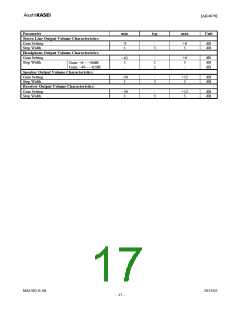
Note 17. Output voltage is proportional to AVDD voltage. Vout = 1.0 x AVDD Vpp(typ)
Note 18. PSRR is referred to SVDD with 200mVpp sine wave.
Note 19. Output voltage is proportional to AVDD voltage. Vout = (LOP) – (LON) = 2.0 x AVDD Vpp(typ)
Note 20. This is a resistance value between output pin and VSS1. When a resistor is connected between output pins, load
resistance for each output pin is half. Therefore, it is necessary to decide load resistance in consideration of
these.
Note 21. This is a capacitance value between output pin and VSS1. When a capacitor is connected between output pins,
load capacitance for each output pin doubles. Therefore, it is necessary to decide load capacitance in
consideration of these.
Note 22. Input signal of left and right channels is same phase and level.
Note 23. Output voltage is proportional to AVDD voltage. Vout = (RCP) – (RCN) = 2.17 x AVDD Vpp(typ)
Po = 15mW @ 32Ω, Vout = 1.96Vpp. Po = 60mW @ 32Ω, Vout = 3.91Vpp.
MS1402-E-06
2013/02
- 15 -

 AKM [ ASAHI KASEI MICROSYSTEMS ]