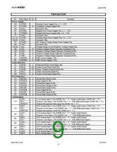
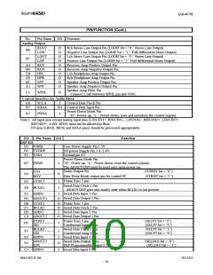
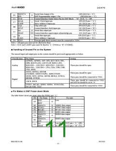
[AK4679]
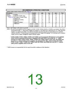
RECOMMENDED OPERATING CONDITIONS
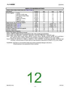
(VSS1=VSS2=VSS3=VSS4=VSS5=0V; Note 4)
Parameter
Power
Supplies
Symbol
AVDD
SVDD
PVDD
DVDD
TVDDA
VDDE
TVDDE
min
1.7
3.0
1.7
1.7
1.6
1.1
1.6
typ
1.8
4.2
1.8
1.8
1.8
1.2
1.8
−
max
2.0
5.5
2.0
2.0
3.6
1.3
3.6
0.2
0.2
0.2
Unit
V
V
V
V
V
V
V
V
Analog
SPK/RCV/LINE-Amp
(Note 9) HP-Amp & Charge Pump
Digital Core
Digital I/O (Codec)
DSP Core
Digital I/O (DSP)
Difference
AVDD – PVDD
AVDD – DVDD
PVDD – DVDD
−0.2
−0.2
−0.2
V
V
−
−
Note 4. All voltages with respect to ground.
Note 9. The power-up sequence between supplies (AVDD, SVDD, PVDD, DVDD or TVDD) is not critical. The PDNA
pin should be held “L” when power supplies are tuning on. The PDNA pin is allowed to be “H” after all power
supplies are applied and settled. The AK4679 should be operated along the recommended power-up/down
sequence shown in “System Design (Grounding and Power Supply Decoupling)” to avoid pop noise at speaker
output, receiver output, headphone outputs and line outputs.
* AVDD, PVDD, DVDD, VDDE, TVDDE and TVDDA can be powered OFF (Power is not applied)
when SVDD is powered ON (Power is applied) with both PDNA and PDNE pin “L”. When
turning on AVDD, PVDD, DVDD, VDDE, TVDDE and TVDDA again in this case, the PDNA pin
must be “L” until all other power supplies are powered ON. Also, when turning off AVDD,
PVDD, DVDD, VDDE, TVDDE and TVDDA both the PDNA and PDNE pin must be “L” before
other power supplies start to turn off.
* AKM assumes no responsibility for the usage beyond the conditions in this datasheet.
MS1402-E-06
2013/02
- 13 -

 AKM [ ASAHI KASEI MICROSYSTEMS ]