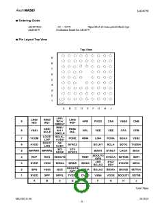
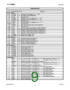
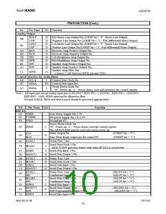
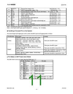
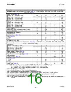
[AK4679]
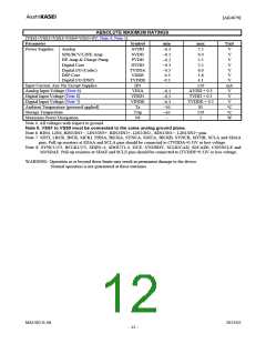
ABSOLUTE MAXIMUM RATINGS
(VSS1=VSS2=VSS3=VSS4=VSS5=0V; Note 4, Note 5)
Parameter
Power Supplies:
Symbol
AVDD
SVDD
PVDD
DVDD
TVDDA
VDDE
TVDDE
IIN
VINA
VIND1
VINDE
Ta
min
max
2.5
6.0
2.5
2.5
6.0
1.6
4.1
Unit
V
V
V
V
V
V
V
mA
V
V
V
°C
°C
W
Analog
−0.3
−0.3
−0.3
−0.3
−0.3
-0.3
-0.3
-
−0.3
−0.3
−0.3
−30
−65
−
SPK/RCV/LINE-Amp
HP-Amp & Charge Pump
Digital Core
Digital I/O (Codec)
DSP Core
Digital I/O (DSP)
Input Current, Any Pin Except Supplies
Analog Input Voltage (Note 6)
Digital Input Voltage (Note 8)
Digital Input Voltage (Note 7)
Ambient Temperature (powered applied)
Storage Temperature
±10
AVDD + 0.3
TVDD + 0.3
TVDDE + 0.3
85
Tstg
Pd
150
1
Maximum Power Dissipation
Note 4. All voltages with respect to ground.
Note 5. VSS1 to VSS5 must be connected to the same analog ground plane.
Note 6. RIN4, LIN4, RIN3/IN3−, LIN3/IN3+, RIN2/IN2+, LIN2/IN2-, RIN1/IN1−, LIN1/IN1+ pins
Note 7. SDTI, LRCK, BICK, MCKI, PDNA, BICKA, SYNCA, SDITA, BICKB, SYNCB, SDTIB, SCLA and SDAA
pins. Pull-up resistors at SDAA and SCLA pins should be connected to (TVDDA+0.3)V or less voltage.
Note 8. SYNC1/2/3, BCLK1/2/3, SDIN1-4, SDOUT1-4, I2CE, STO/RDY, SCLK/CAD, SI/CAD0, CSN/SCLE and
SO/SDAE. Pull-up resistors at SDAE and SCLE pins should be connected to (TVDDE+0.3)V or less voltage.
WARNING: Operation at or beyond these limits may result in permanent damage to the device.
Normal operation is not guaranteed at these extremes.
MS1402-E-06
2013/02
- 12 -

 AKM [ ASAHI KASEI MICROSYSTEMS ]