[AK4679]
Serial Control Interface (SPI, I2C-bus)
■ General
Audio Block is controlled by I2C bus only while DSP Block is controlled by the SPI or I2C bus which is set by I2CE pin
state.
■ Serial Control Interface (I2C-bus)
The AK4679 supports the fast-mode I2C-bus (max: 400 kHz). Pull-up resistors at SDAA and SCLA pins must be
connected to (TVDDA+0.3)V or less voltage. Pull-up resistors at SDAE and SCLE pins must be connected to
(TVDDE+0.3)V or less voltage.
SCLA and SCLE are denoted by SCL. SDAA and SDAE are denoted by SDA in this document.
(2)-1. WRITE Operations
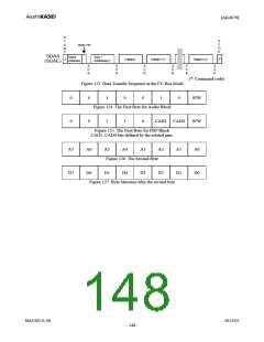
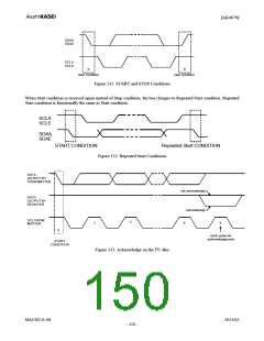
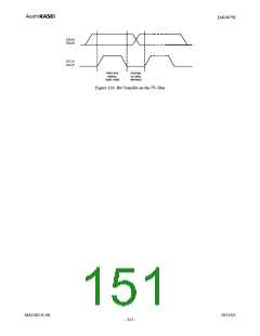
Figure 123 shows the data transfer sequence for the I2C-bus mode. All commands are preceded by a START condition. A
HIGH to LOW transition on the SDA line while SCL is HIGH indicates a START condition (Figure 131). After the
START condition, a slave address is sent. This address is 7 bits long followed by the eighth bit that is a data direction bit
(R/W). The most significant seven bits of the slave address are shown in Figure 124 and Figure 125. If the slave address
matches that of the AK4679, the AK4679 generates an acknowledge and the operation is executed. The master must
generate the acknowledge-related clock pulse and release the SDA line (HIGH) during the acknowledge clock pulse
(Figure 133). A R/W bit value of “1” indicates that the read operation is to be executed. A “0” indicates that the write
operation is to be executed.
The second byte consists of the control register address of the AK4679. When accesing the PRAM, CRAM and OFFREG
the second byte consists command code at this time. This address is 8bits and the format is MSB first (Figure 126). The
data after the second byte contains control data. The format is MSB first, 8bits (Figure 127). The AK4679 generates an
acknowledge after each byte is received. A data transfer is always terminated by a STOP condition generated by the
master. A LOW to HIGH transition on the SDA line while SCL is HIGH defines a STOP condition (Figure 131).
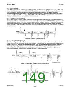
The AK4679 can perform more than one byte write operation per sequence. After receipt of the third byte the AK4679
generates an acknowledge and awaits the next data. The master can transmit more than one byte instead of terminating the
write cycle after the first data byte is transferred. After receiving each data packet the internal 8-bit address counter is
incremented by one, and the next data is automatically taken into the next address. If the address for CODEC registers
exceeds AFH prior to generating a stop condition, the address counter will “roll over” to 00H and the previous data will be
overwritten.
The data on the SDA line must remain stable during the HIGH period of the clock. The HIGH or LOW state of the data
line can only change when the clock signal on the SCL line is LOW (Figure 134) except for the START and STOP
conditions.
MS1402-E-06
2013/02
- 147 -

 AKM [ ASAHI KASEI MICROSYSTEMS ]