[AK4679]
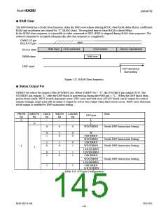
■ RAM Clear
The DSP block has a RAM clear function. After the DSP reset release (during RUN), data RAM, delay RAM, coefficient
RAM and accelerator are cleared by “0” (RAM clear). The required time to clear RAM is about 400µs.
In the RAM clear sequence, it is possible to order command to DSP. (DSP is stopped during RAM clear sequence. The
ordered command is accepted automatically after this sequence is completed.)
SYNC1/3 pin
BCLK1/3 pin
Input
Wait Sync CGU unlocked
CGU locked
Device Operational
Device state
RAM clear
RAM clear
DSP start
DSP Operational
Start working
Figure 122. RAM Clear Sequence
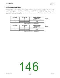
■ Status Output Pin
STRDY bit selects the output of the STO/RDY pin. When STRDY bit = “0”, the STO/RDY pin outputs STO. The
STO/RDY pin outputs “L” after the DSP block is powered-up during the PDN pin = “L”. When the DSP block exits
power-down mode, WDT (watch dog timer) error, CRC error and lock error of CGU block can be output by control
register settings. Each error OR’ed status is output by active-low output when these errors occur. WDT error detection
result output is enabled by DSP instruction setting.
PWSW MRSTN CRCE
WDTN
bit
LOCKE
Note
STO pin
bit
bit
bit
bit
0
-
0
--
--
--
L
L
0
0
0
WDTERRN
Needs DSP Instruction Setting
0
1
1
0
0
0
H
CRCERRN
WDTERRN
CRCERRN
WDTERRN
Needs DSP Instruction Setting
Needs DSP Instruction Setting
1
0
1
0
0
1
1
1
LOCKERRN
LOCKERRN
CRCERRN
0
1
1
0
1
1
WDTERRN
LOCKERRN
CRCERRN
Needs DSP Instruction Setting
1
1
1
LOCKERRN
Table 129. STO pin Configuration
MS1402-E-06
2013/02
- 145 -

 AKM [ ASAHI KASEI MICROSYSTEMS ]