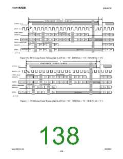
[AK4679]
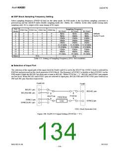
■ DSP Block Sampling Frequency Setting
Select sampling frequency (FSD[3:0] bits) on the sleep mode. In FSD mode 6, the Up-Down sampling converter is
powered-up and the AK4679 enters double sampling mode (fs1 =8kHz, fs2 =16kHz). In the other modes (using unity
sampling rate), fs2 is output at the same timing of fs1 input.
FSD
Mode
Sampling Frequency
fs2 Port2
8kHz
FSD3 bit FSD2 bit FSD1 bit FSD0 bit
fs1 Port1
8kHz
8kHz
12kHz
16kHz
24kHz
fs3 Port3
8kHz
(default)
0
6
1
2
3
0
0
0
0
0
0
0
1
1
1
0
1
0
0
0
1
1
0
0
1
0
1
0
1
1
0
1
1
1
1
0
0
1
0
1
1
1
0
1
1
Double FS mode
16kHz
12kHz
16kHz
24kHz
8kHz
12kHz
16kHz
24kHz
11.025kHz
22.05kHz
32kHz
48kHz
44.1kHz
5
7
11.025kHz
22.05kHz
32kHz
11.025kHz
22.05kHz
32kHz
10
11
15
Others
48kHz
44.1kHz
48kHz
44.1kHz
N/A
N/A
Table 123. Setting of Sampling Frequency (N/A: Not available)
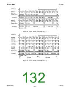
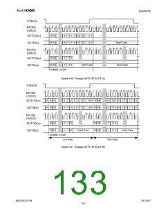
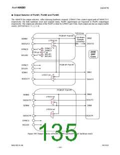
■ Selection of Input Port
The selection of the signal path of the input clock for Port#1 and #3 is set by the SELPT bit. SYNC2 clock is selected by
FSD bits and processed on the clock generator (CGU) block. The frequency of SYNC2 is double as that of SYNC1 on the
FSD mode 6 while the BCLK2 bit clock rate is same as BCLK1. When PT2N bit = “1”, BCLK2 and SYNC2 pin outputs
are low level. When BCLK1 and SYNC1 pins are selected as input pins, BCLK3/JX0 and SYNC3/JX1 pins could act as
JX0 and JX1 pins function respectively.
Port#1,#3
Port#2
BCLK1 pin
BCLK2 pin
BCLK3/JX0 pin
PT2N bit
SELPT bit
FSD[3:0] bit
CGU
SYNC1 pin
SYNC2 pin
SYNC3/JX1 pin
CGU: Clock Generator Unit
Figure 108. Port#1/2/3 Signal Setting (PT2N bit = “0”)
MS1402-E-06
2013/02
- 134 -

 AKM [ ASAHI KASEI MICROSYSTEMS ]