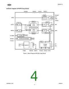
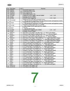
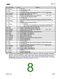
[AK4675]
No. Pin Name
H1 TEST2
I/O
-
Function
Test 2 Pin
This pin must be open.
No Connect Pin
H3 NC
-
No internal bonding. This pin must be opened or connected to the ground.
K3 AVDDA
K4 VSS1A
-
-
HP/SPK-Amp Analog Power Supply Pin
HP/SPK-Amp Ground 1 Pin
2.6V ~ 3.6V
HP/SPK-Amp Digital Interface Power Supply Pin
This pin must be connected to DVDD.
No Connect Pin
No internal bonding. This pin must be opened or connected to the ground.
HP/SPK-Amp External Clock Input Pin (Internal Pull-down pin to VSS1A: typ.
100kΩ)
1.6V ~ 3.6V
H8 TVDDA
J6 NC
-
-
I
K8 MCKIA
HP/SPK-Amp Power-Down Mode Pin
“H”: Power-up
J9 PDNA
I
“L”: Power-down, reset and initializes the control registers for HP/SPK-Amp. “L”
time of 150ns or more after power-up is needed to reset the AK4675.
Positive Charge Pump Capacitor Terminal Pin
H10 CP
H9 CN
O
I
Negative Charge Pump Capacitor Terminal Pin
F10 PVDDA
G10 VSS3A
E9 PVEE
E10 HPL
-
-
Charge Pump Circuit Positive Power Supply Pin
HP/SPK-Amp Ground 3 Pin
Charge Pump Circuit Negative Voltage Output Pin
Lch Headphone-Amp Output Pin
Rch Headphone-Amp Output Pin
Battery Monitor Input Pin
Battery Monitor Output Pin
HP/SPK-Amp Analog Common Voltage Output Pin
Rch HP-Amp Input Pin
2.6V ~ 3.6V
O
O
O
I
O
O
I
B10 HPR
A7 VBATIN
C9 VBATO
C8 VCOMA
C6 RIN1A
A2 LIN1A
I
Lch HP-Amp Input Pin
No Connect Pin
D2 NC
C1 NC
-
-
No internal bonding. This pin must be opened or connected to the ground.
No Connect Pin
No internal bonding. This pin must be opened or connected to the ground.
D1 SVDDA
E1 VSS2A
G1 SPP
-
-
O
O
Speaker-Amp Power Supply Pin
HP/SPK-Amp Ground 2 Pin
Positive Speaker-Amp Output Pin
Negative Speaker-Amp Output Pin
TEST Pin
3.0V ~ 5.5V
F2 SPN
J3 TEST3
K2 SPIN
-
I
This pin must be open.
Speaker-Amp Input Pin
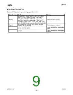
Note 1. All input pins except analog input pins (MDT, LIN1/IN1+, RIN1/IN1−, LIN2/IN2+, RIN2/IN2−, LIN3/IN3+,
RIN3/IN3−, LIN4/IN4+, RIN4/IN4−, SAIN1, SAIN2, SAIN3, LIN1A, RIN1A, SPIN, VBATIN) must not be left
floating. I/O pins except the SDA pin (LRCK, BICK, SYNCA, BICKA, SYNCB, BICK) must be processed
appropriately as shown in “Master Mode/Slave Mode” and “PCM I/F Master Mode/Slave Mode”. The PDA pin
should be pulled-up externally and connected to (DVDD+0.3)V or less.
MS0963-E-00
2008/05
- 8 -

 AKM [ ASAHI KASEI MICROSYSTEMS ]