[AK4634]
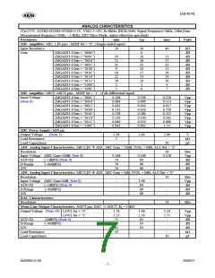
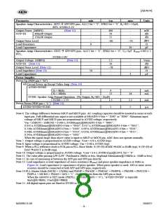
Parameter
min
typ
max
Units
Speaker-Amp Characteristics: SDTI Æ SPP/SPN pins, ALC2 bit = “0”, SPKG bit = “0”, RL=8Ω + 10μH,
BTL, SVDD=3.3V
Output Power (0dBFS)
S/(N+D) 400mW Output
150mW Output
(Note 11)
-
-
-
400
20
-
-
-
mW
dB
55
dB
Output Noise Level
Load Resistance
Load Capacitance
-
8
-
dBV
Ω
pF
−80
-
-
−70
-
30
Speaker-Amp Characteristics: SDTI Æ SPP/SPN pins, ALC2 bit = “0”, SPKG bit = “0”, CL=3μF, Rseries=10Ω x 2,
BTL,
SVDD=3.8V
Output Voltage (0dBFS)
S/(N+D) (Note 12)
(Note 11)
-
-
-
50
-
2.5
20
−78
-
-
-
-
-
3
Vrms
dB
dBV
Ω
Output Noise Level (Note 12)
Load Impedance (Note 13)
Load Capacitance
-
μF
Power Supplies
Power Up (PDN pin = “H”)
All Circuit Power-up Except Video Amp: (Note 14)
AVDD+DVDD
fs = 8kHz
-
-
9
12
-
18
mA
mA
fs = 48kHz
SVDD: Speaker-Amp Normal Operation (No Output, RL=8Ω + 10μH)
SVDD = 3.3V
Power Down (PDN pin = “L”) (Note 15)
AVDD+DVDD+SVDD
-
1.5
2.5
5
mA
-
1
μA
Note 6. The voltage difference between MICP and MICN pins. AC coupling capacitor should be inserted in series at each
input pin. Full-differential mic input is not available at MGAIN3-0 bits = “1000” or “0000”. Maximum input
voltage of MICP and MICN pins are proportional to AVDD voltage, respectively.
Vin = |(MICP) − (MICN)| = 0.069 x AVDD(max)@MGAIN3-0 bits = “0001”,
0.035 x AVDD(max)@MGAIN3-0 bits = “0010”, 0.017 x AVDD(max)@MGAIN3-0 bits = “0011”,
0.218x AVDD(max)@MGAIN3-0 bits = “0100”, 0.097x AVDD(max)@MGAIN3-0 bits = “0101”,
0.048x AVDD(max)@MGAIN3-0 bits = “0110”, 0.024x AVDD(max)@MGAIN3-0 bits = “0111”,
0.345x AVDD(max)@MGAIN3-0 bits = “1001”
When the signal larger than above value is input to MICP or MICN pin, ADC does not operate normally.
Note 7. Output voltage is proportional to AVDD voltage. Vout = 0.8 x AVDD (typ)
Note 8. Input voltage is proportional to AVDD voltage. Vin = 0.06 x AVDD (typ)
Note 9. When a PLL reference clock is FCK pin in PLL Slave Mode, S/ (N+D) of MICÆADC is 81dB (typ), S/ (N+D) of
DACÆAOUT is 81dB (typ).
Note 10. Output voltage is proportional to AVDD voltage. Vout = 0.6 x AVDD (typ)@LOVL bit = “0”.
Note 11. The value after passing LPF (LPF : Passband is 20kHz or less, Stopband Attenuation@250kHz is –50dB or less)
Note 12. In case of measuring at between the SPP pin and SPN pin directly.
Note 13. Load impedance is total impedance of series resistance (Rseries) and piezo speaker impedance at 1kHz in
Figure 44. Load capacitance is capacitance of piezo speaker. When piezo speaker is used, 10Ω or more series
resistors should be connected at both SPP and SPN pins, respectively.
Note 14.PLL Master Mode (MCKI = 12MHz) and PMMP = PMADC = PMDAC = PMPFIL = PMSPK = PMVCM =
PMPLL = MCKO = PMAO = M/S = “1”. Output current from the MPI pin is 0mA.
When the AK4634 is EXT mode (PMPLL = MCKO = M/S = “0”), “AVDD+DVDD” is typically
6mA@fs=8kHz, 11mA@fs=48kHz
Note 15. All digital inputs pins are fixed to DVDD or VSS2.
MS0983-E-00
2008/07
- 8 -

 AKM [ ASAHI KASEI MICROSYSTEMS ]