[AK4634]
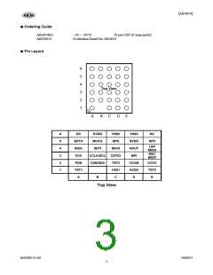
PIN/FUNCTION
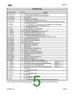
No. Pin Name
D2 VCOM
I/O
O
Function
Common Voltage Output Pin, 0.45 x AVDD
Bias voltage of ADC inputs and DAC outputs.
Ground Pin
C1
D1
VSS1
-
-
AVDD
Analog Power Supply Pin
Output Pin for Loop Filter of PLL Circuit
This pin must be connected to VSS1 with one resistor and capacitor in series.
Power-Down Mode Pin
E2
VCOC
O
A2
“H”: Power up, “L”: Power down reset and initialize the control register.
AK4634 must always be reset upon power-up.
Control Mode Select Pin
PDN
I
A6 I2C
I
I
“H”: I2C Bus, “L”: 3-wire Serial
CSN
B2
Chip Select Pin (I2C pin = “L”)
I/O Control Data Input/Output Pin (I2C pin = “H”)
SDA
CCLK
SCL
I
I
Control Data Clock Pin (I2C pin = “L”)
Control Data Clock Pin (I2C pin = “H”)
B3
Control Data Input/Output Pin (I2C pin = “L”)
This pin must be connected to the ground. (I2C pin = “H”)
C3 CDTIO
I/O
B4
A5
A3
A4
B6
C6
C4
B5
E5
C5
D6
D5
D4
D3
SDTI
SDTO
FCK
I
Audio Serial Data Input Pin
Audio Serial Data Output Pin
O
I/O Frame Clock Pin
BICK
DVDD
VSS2
MCKI
MCKO
SPP
I/O Audio Serial Data Clock Pin
-
-
Digital Power Supply Pin
Ground Pin.
External Master Clock Input Pin
Master Clock Output Pin
I
O
O
O
-
Speaker Amp Positive Output Pin
Speaker Amp Negative Output Pin
Ground Pin
SPN
VSS3
SVDD
AOUT
MPI
-
Speaker Amp Power Supply Pin
Mono Line Output Pin
O
O
I
MIC Power Supply Pin for Microphone
Microphone Input Pin for Single Ended Input
Microphone Positive Input Pin for Differential Input
Line Input Pin for Single Ended Input
Microphone Negative Input Pin for Differential Input
TEST3 pin
MIC
(MDIF bit = “0”)
(MDIF bit = “1”)
(MDIF bit = “0”)
(MDIF bit = “1”)
E3
E4
MICP
LIN
I
I
MICN
I
E1
C2
A1
E6
TST3
TST2
TST1
NC
-
-
-
-
This pin must be open.
TEST2 pin
This pin must be open.
TEST1 pin
This pin must be open.
No Connection.
No internal bonding. This pin must be connected to the ground.
Note : All input pins except analog input pins (MIC/MICP, LIN/MICN pins) must not be left floating
MS0983-E-00
2008/07
- 5 -

 AKM [ ASAHI KASEI MICROSYSTEMS ]