ASAHI KASEI
[AK4115]
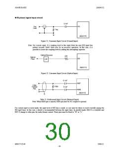
Bi-phase signal output circuit
The AK4115 includes two TX output buffers. The output level is proportional to TVDD voltage. The T1 in Figure 23,
Figure 24, Figure 25 and Figure 26 is a transformer of 1:1. The resistor values should use ±1% accuracy.
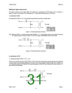
1. Line Driver of TX0
The output level of TX0 is 0.5V 20% using the external resistor network in consumer mode.
±
R1
TX0
Ω
75 cable
R2
TVDD R1
R2
TVSS
3.3V 240Ω 150Ω
3.0V 220Ω 150Ω
5.0V 430Ω 150Ω
T1
Figure 23. TX0 External Resistor Network 1
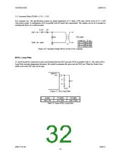
Note: When the AK4115 is in the power-down mode (PDN pin = “L”), power supply current can be reduced by using an
AC coupling capacitor as shown in Figure 24, since TX1 output is undetermined in power-down mode.
0.1uF
R1
TX0
75Ω cable
R2
TVDD R1
R2
Ω
Ω
Ω
Ω
Ω
Ω
3.3V
3.0V
5.0V
240
220
430
150
150
150
TVSS
T1
Figure 24. TX0 External Resistor Network 2
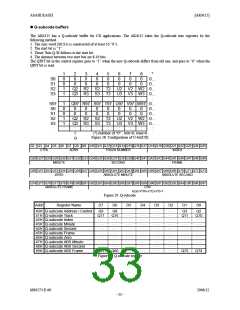
2. Line Driver of TX1
2-1. Professional Mode (TVDD = 4.5V ∼ 5.5V)
The TX1 has an RS422 line driver when TVDD is 5V±10%. The AES3 specification states that the line driver shall have
a balanced output with an internal impedance of 110 ohms ±20% and also requires a balanced output drive capability of 2
to 7 volts peak-to-peak into 110 ohm load. The internal impedance of the RS422 driver along with a series resistors of 75
ohms realizes this requirement.
75Ω
0.1uF
TXP1
TXN1
110Ω cable
T1
Figure 25. Professional Output Driver Circuit
MS0573-E-00
2006/12
- 31 -

 AKM [ ASAHI KASEI MICROSYSTEMS ]