The 14.8 dBm output power (P
also makes the MGA-81563
extremely useful for pre-driver,
driver and buffer stages. For
)
Specifications and Statistical
Parameters
Several categories of parameters
appear within this data sheet.
1dB
MGA-81563 Applications
Information
Introduction
transmitter gain stage applications Parameters may be described with
This high performance GaAs
MMIC amplifier was developed for
commercial wireless applications
from 100 MHz to 6 GHz.
that require higher output power,
the MGA-81563 can provide
50 mW(17dBm)ofsaturated
output power with a high power
added efficiency of 45%.
values that are either “minimum
or maximum,” “typical,” or
“standard deviations.”
The values for parameters are
based on comprehensive product
characterization data, in which
automated measurements are
made on of a minimum of
500 partstakenfrom3non-
consecutive process lots of
semiconductor wafers. The data
derived from product character-
ization tends to be normally
distributed, e.g., fits the standard
“bell curve.”
The MGA-81563 runs on only
3 volts and typically requires only
42 mA to deliver 14.8 dBm of
output power at 1 dB gain
compression.
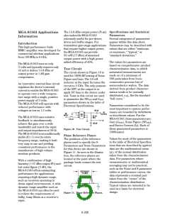
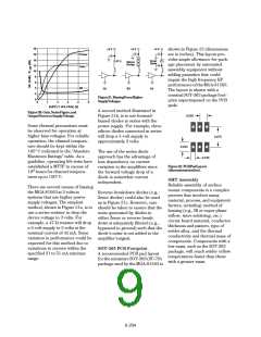
Test Circuit
The circuit shown in Figure 10 is
used for 100% RF testing of Noise
Figure and Gain. The 3.9 nH
inductor at the input fix-tunes the
circuit to 2 GHz. The only purpose
of the RFC at the output is to
apply DC bias to the device under
test. Tests in this circuit are used
An innovative internal bias circuit
regulates the device’s internal
current to enable the MGA-81563
to operate over a wide tempera-
ture range with a single, positive
power supply of 3 volts.
The MGA-81563 will operate with
reduced performance with
voltages as low as 1.5 volts.
to guarantee the NF
and G
test
test
parameters shown in the table of
Electrical Specifications.
Parameters considered to be the
most important to system perfor-
mance are bounded by minimum
or maximum values. For the
100 pF
RF
RF
INPUT
OUTPUT
22 nH
RFC
The MGA-81563 uses resistive
feedback to simultaneously
achieve flat gain over a wide
bandwidth and match the input
and output impedances to 50 Ω.
The MGA-81563 is unconditionally
stable (K>1) over its entire
frequency range, making it both
very easy to use and yielding
consistent performance in the
manufacture of high volume
wireless products.
MGA-81563,theseparametersare:
3.9 nH
Vd
Gain (G ), Noise Figure (NF ),
test
test
100 pF
and Device Current (I ). Each of
d
these guaranteed parameters is
100%tested.
Figure 10. Test Circuit.
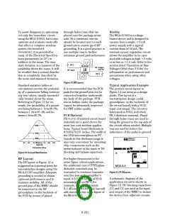
Phase Reference Planes
The positions of the reference
planes used to specify the S-
Parameters and Noise Parameters
for this device are shown in
Figure 11. As seen in the illustra-
tion, the reference planes are
located at the point where the
package leads contact the test
circuit.
Values for most of the parameters
in the table of Electrical Specifica-
tions that are described by typical
data are the mathematical mean
(µ), of the normal distribution
taken from the characterization
data. For parameters where
measurements or mathematical
averaging may not be practical,
such as the Noise and S-parameter
tables or performance curves, the
data represents a nominal part
taken from the “center” of the
characterization distribution.
Typical values are intended to be
used as a basis for electrical
design.
With a combination of high
linearity (+27 dBm output IP ) and
3
low noise figure (3 dB), the
MGA-81563offersoutstanding
performance for applications
requiring a high dynamic range,
such as receivers operating in
dense signal environments. A wide
dynamic range amplifier such as
the MGA-81563 can often be used
to relieve the requirements of
bulky, lossy filters at a receiver’s
input.
REFERENCE
PLANES
TEST CIRCUIT
Figure 11. Phase Reference Planes.
6-200

 AGILENT [ AGILENT TECHNOLOGIES, LTD. ]