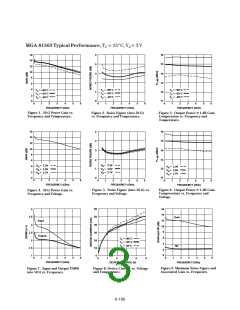
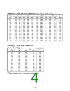
Although the input terminal of the bias lines that could cause oscilla- The input of the MGA-81563 is
MGA-81563 is at ground potential, tion. C4 will not normally be
it is not a current sink. If the input needed unless several stages are
partially matched internally to
50 Ω.Withoutexternalmatching
elements, the input VSWR of the
MGA-81563is3.0:1at300MHz
and decreases to 1.5:1 at 6 GHz.
This will be adequate for many
applications. If a better input
is connected to a preceding stage
cascaded using a common power
that has a voltage present, the use supply.
of the DC blocking capacitor (C1)
is required.
When multiple bypass capacitors
are used, consideration should be
given to potential resonances. It is VSWR is required, the use of a
C2
V
d
C4
important to ensure that the
capacitors when combined with
additional parasitic L’s and C’s on
the circuit board do not form
resonant circuits. The addition of
a small value resistor in the bias
supply line between bypass
capacitors will often “de-Q” the
bias circuit and eliminate the
effect of a resonance.
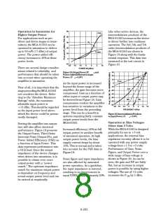
series inductor, L1 in the applica-
tions example, (or, alternatively a
length of high impedance trans-
mission line) is all that is needed
to improve the match. The table in
Figure 16 shows suggested values
for L1 for various wireless fre-
quency bands.
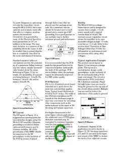
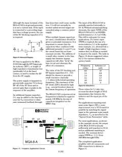
RFC
C2
RF
Input C1
RF
Output
L1
Figure15.SchematicDiagram.
DC bias is applied to the MGA-
81563 through the RF Output pin.
An inductor (RFC), or length of
high impedance transmission line
(preferably λ/4 at the band
Frequency
(GHz)
Inductor, L1
(nH)
The value of the DC blocking and
RF bypass capacitors (C1– C3)
should be chosen to provide a
small reactance (typically
< 5 ohms)atthelowestoperating
frequency. The reactance of the
RF choke (RFC) should be high
(e.g., several hundred ohms) at
the lowest frequency of operation.
0.9
1.5
1.9
2.4
4.0
5.8
10
6.8
3.9
2.7
0.5
0
center), is used to isolate the RF
from the DC supply.
The power supply is bypassed to
ground with capacitor C3 to keep
RF off of the DC lines and to
prevent gain dips or peaks in the
response of the amplifier.
Figure16.ValuesforL1.
These values for L1 take into
account the short length of 50 Ω
transmission line between the
inductor and the input pin of the
device.
The MGA-81563’s response at low
frequencies is limited to approxi-
mately 100 MHz by the size of
capacitors integrated on the
MMIC chip.
An additional bypass capacitor,
C4, may be added to the bias line
near the V connection to elimi-
d
nate unwanted feedback through
For applications requiring mini-
mum noise figure (NF ), some
o
improvement over a 50 Ω match is
possible by matching the signal
input to the optimum noise match
H
impedance, Γ , as specified in the
o
“Typical Noise Parameters” table.
OUT
C1
L1
For most applications, as shown
in the example circuit, the output
of the MGA-81563 is already
sufficiently well matched to 50 Ω
and no additional matching is
needed. The nominal device
outputVSWRis≤ 2.2:1from
300 MHzthrough6GHz.
C2
IN
RFC
C3
+V
C4
The completed application
amplifier with all components and
SMA connectors is shown in
Figure17.
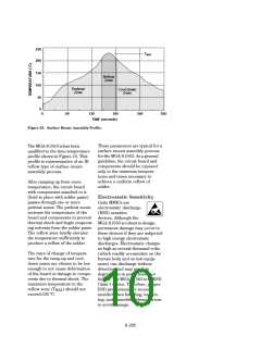
MGA-8-A
Figure 17. Complete Application Circuit.
6-202

 AGILENT [ AGILENT TECHNOLOGIES, LTD. ]