2
Absolute Maximum Ratings[1] TC = +25°C
Symbol Parameter
Unit
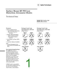
SOT-23
SOT-323
If
Forward Current (1 µs Pulse) Amp
1
Same as VBR
150
1
Same as VBR
150
PIV
Tj
Peak Inverse Voltage
Junction Temperature
Storage Temperature
Thermal Resistance[2]
V
°C
°C
Tstg
θjc
-65 to 150
500
-65 to 150
150
°C/W
Notes:
1. Operation in excess of any one of these conditions may result in permanent damage to
the device.
2.
T
C = +25°C, where TC is defined to be the temperature at the package pins where
contact is made to the circuit board.
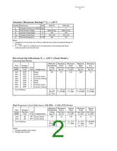
Electrical Specifications TC = +25°C (Each Diode)
Conventional Diodes
Minimum
Breakdown
Voltage
Maximum
Total
Maximum
Total
Minimum
High
Maximum
Low
Part
Package
Number Marking Lead
Resistance Capacitance Resistance Resistance
HSMP-
Code
Code Configuration
V
BR (V)
RT (Ω)
CT (pF)
RH (Ω)
RL (Ω)
3810
3812
3813
3814
381B
381C
381E
381F
E0[1]
E2[1]
E3[1]
E4[1]
E0[2]
E2[2]
E3[2]
E4[2]
0
2
3
Single
Series
Common Anode
Common Cathode
Single
Series
Common Anode
Common Cathode
100
3.0
0.35
1500
10
4
B
C
E
F
Test Conditions
VR = VBR
Measure
IR ≤ 10 µA
IF = 100 mA
f = 100 MHz
VR = 50 V
f = 1 MHz
IR = 0.01 mA IF = 20 mA
f = 100 MHz f= 100 MHz
High Frequency (Low Inductance, 500 MHz – 3 GHz) PIN Diodes
Minimum
Breakdown
Voltage
Maximum
Series
Typical
Total
Maximum
Total
Typical
Total
Part
Package
Number Marking Lead
Resistance Capacitance Capacitance Inductance
HSMP-
Code
Code Configuration
VBR (V)
RS (Ω)
CT (pF)
CT (pF)
LT (nH)
4810
481B
EB
EB
B[1] Dual Cathode
B[2] Dual Cathode
100
3.0
0.35
0.4
1.0
Test Conditions
VR = VBR
Measure
IR ≤ 10 µA
IF = 100 mA
VR = 50 V
f = 1 MHz
VR = 50 V
f = 1 MHz
VR = 0 V
f = 500 MHz–
3 GHz
Notes:
1. Package marking code is white.
2. Package laser marked.

 AGILENT [ AGILENT TECHNOLOGIES, LTD. ]