Recommended Application Circuit Components
Component
Recommended Value
6.2 Ω ± 5%, 0.5 Watt, for 2.7 ≤ V ≤ 3.6 V operation
R1
CC
15.0 Ω ± 5%, 0.5 Watt, for 4.75 ≤ V ≤ 5.25 V operation
CC
[4]
CX1
0.47 µF ± 20%, X7R Ceramic
6.8 µF ± 20%, Tantalum
[5]
CX2
Notes:
4. CX1 must be placed within 0.7 cm of the HSDL-3612 to obtain optimum noise immunity.
5. In "HSDL-3612 Functional Block Diagram" on page 1 it is assumed that Vled and V share the same supply
CC
voltage and filter capacitors. In case the 2 pins are powered by different supplies CX2 is applicable for Vled and
CX1 for V . In environments with noisy power supplies, including CX2 on the V line can enhance supply
CC
CC
rejection performance.
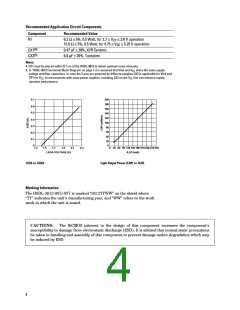
0.7
0.6
0.5
200
180
160
140
120
100
80
0.4
0.3
0.2
0.1
0
60
40
20
0
1.3
1.5
1.7
1.9
2.1
2.3
0
30 60 90 120 150 180 210 240 270 300
ILED (mA)
LEDA VOLTAGE (V)
ILED vs. LEDA.
Light Output Power (LOP) vs. ILED.
Marking Information
The HSDL-3612-007/-037 is marked “3612YYWW” on the shield where
“YY” indicates the unit’s manufacturing year, and “WW” refers to the work
week in which the unit is tested.
CAUTIONS: The BiCMOS inherent to the design of this component increases the component’s
susceptibility to damage from electrostatic discharge (ESD). It is advised that normal static precautions
be taken in handling and assembly of this component to prevent damage and/or degradation which may
be induced by ESD.
4

 AGILENT [ AGILENT TECHNOLOGIES, LTD. ]