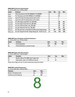
HDMP-0452 AC Electrical Specifications
T = 0°C to +70°C, V = 3.15 V to 3.45 V
A
CC
Symbol
Parameter
Units
ns
Min.
Typ.
4.0
Max.
t
t
t
t
t
t
t
t
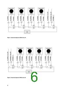
Total Loop Latency from FM_NODE[0] to TO_NODE[0]
Per Cell Latency from FM_NODE[4] to TO_NODE[0]
Input LVTTL Rise Time Requirement, 0.8 V to 2.0 V
Input LVTTL Fall Time Requirement, 2.0 V to 0.8 V
HS_OUT Single-Ended Rise Time, 20%-80%
delay1
ns
0.8
delay2
ns
2
r,LVTTLin
f,LVTTLin
rs,HS_OUT
fs,HS_OUT
rd,HS_OUT
fd,HS_OUT
ns
2
ps
200
200
200
200
1200
1400
350
HS_OUT Single-Ended Fall Time, 20%-80%
ps
350
HS_OUT Differential Rise Time, 20%-80%
ps
350
HS_OUT Differential Fall Time, 20%-80%
ps
350
V
V
HS_IN Input Peak-to-Peak Required Differential Voltage Range
HS_OUT Output Pk-Pk Diff. Voltage Range (Z0 = 75 Ohm, Fig. 9)
mV
mV
200
2000
2000
IP,HS_IN
1100
OP,HS_OUT
HDMP-0452 Power Dissipation and Thermal Resistance
T = 0°C to +70°C, V = 3.15 V to 3.45 V
A
CC
Symbol
Parameter
Units
Typ.
Max.
P
Power Dissipation
mW
660
7
950
D
Θ
Thermal Resistance, Junction to Case
°C/W
jc
HDMP-0452 Output Jitter Characteristics
T = 0°C to +70°C, V = 3.15 V to 3.45 V
A
CC
Symbol
Parameter
Units
ps
Typ.
5
Max.
RJ
DJ
Random Jitter at TO_NODE pins (1 sigma rms)
Deterministic Jitter at TO_NODE pins (pk-pk)
ps
20
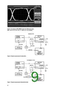
Please refer to Figures 6 and 7 for jitter measurement setup information.
HDMP-0452 Locking Characteristics
T = 0°C to +70°C, V = 3.15 V to 3.45 V
A
CC
Parameter
Units
bits
µs
Max.
2500
500
Bit Sync Time (phase lock)
Frequency Lock at Powerup
8

 AGILENT [ AGILENT TECHNOLOGIES, LTD. ]