Electrical Description
The electrical configuration of
these CMOS IC alphanumeric
displays allows for an effective
interface to a display controller
circuit that supplies decoded
character information. The row
data for a given column (one 7
bit byte per character) is loaded
(bit serial) into the on-board 28
bit shift register with high to
low transitions of the Clock
input. To load decoded
shifting the character 4 data
over one character position.
This process is repeated for the
other two characters until all 28
bits of column data (four 7 bit
bytes of character column data)
are loaded into the on-board
shift register. Then the column
1 input, VCOL pin 1, is
energized to illuminate column
1 in all four characters. This
process is repeated for columns
2, 3, 4 and 5. All VCOL inputs
should be at logic low to insure
the display is off when loading
data. The display will be
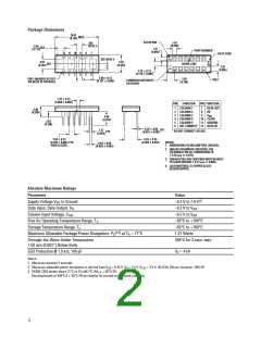
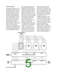
The display contains four 5 x 7
LED dot matrix characters and
two CMOS integrated circuits,
as shown in Figure 1. The two
CMOS integrated circuits form
an on-board 28 bit serial-in/
parallel-out shift register that
will accept standard TTL logic
levels. The Data Input, pin 12,
is connected to bit position 1
and the Data Output, pin 7, is
connected to bit position 28.
The shift register outputs
control constant current sinking
LED row drivers. A logic 1
stored in the shift register
enables the corresponding LED
row driver and a logic 0 stored
in the shift register disables the
corresponding LED row driver.
character information into the
display, column data for
character 4 is loaded first and
the column data for character 1
is loaded last in the following
manner. The 7 data bits for
column 1, character 4, are
loaded into the on-board shift
register. Next, the 7 data bits
for column 1, character 3, are
loaded into the shift register,
blanked when the blanking
input VB, pin 8, is at logic low
regardless of the outputs of the
shift register or whether one of
the VCOL inputs is energized.
Refer to Application Note 1016
for drive circuit information.
COLUMN DRIVE INPUTS
COLUMN
1
2 3 4 5
LED
MATRIX
2
LED
MATRIX
3
LED
MATRIX
4
ROWS 1-7
ROWS 1-7
ROWS 1-7
1
2 3 4 5 6 7
ROWS
BLANKING
CONTROL, V
CONSTANT CURRENT SINKING LED DRIVERS
B
ROWS 8-14
ROWS 15-21
ROWS 22-28
1
2
3
4
5 6 7
SERIAL
DATA
INPUT
SERIAL
DATA
OUTPUT
28-BIT SIPO SHIFT REGISTER
CLOCK
Figure 1. Display block diagram.
5

 AGILENT [ AGILENT TECHNOLOGIES, LTD. ]