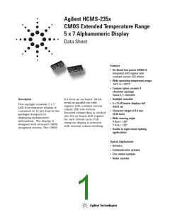
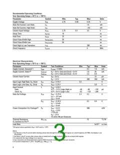
Recommended Operating Conditions
Over Operating Range (–55°C to + 100°C)
Parameter
Symbol
Min.
Typ.
Max
5.25
1.±
Units
V
Supply Voltage
VDD
4.75
5.00
Data Out Current, Low State
Data Out Current, High State
Column Input Voltage
Setup Time
IOL
mA
mA
V
IOH
–0.5
3.5
VCOL
2.75
10
3.0
tSETUP
tHOLD
tWH(CLOCK)
tWL(CLOCK)
tTHL
ns
Hold Time
25
ns
Clock Pulse Width High
Clock Pulse Width Low
Clock High to Low Transition
Clock Frequency
50
ns
50
ns
200
5
ns
fCLOCK
MHz
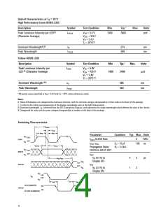
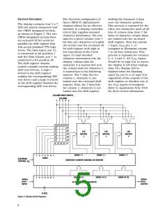
Electrical Characteristics
Over Operating Range (–55°C to + 100°C)
Parameter
Supply Current, Dynamic[1]
Supply Current, Static[2]
Symbol
IDDD
Test Conditions
fCLOCK = 5 MHz
Min
Typ.*
±.2
Max
7.8
Units
mA
mA
IDDDSoff
IDDDSon
VB = 0.4 V, Data and Clock = 0.4 V
VB = 2.4 V, Data and Clock = 0.4 V
1.8
2.2
2±
±.0
Column Input Current
ICOL
VB = 0.4 V
10
µA
mA
V
VB = 2.4 V
500
±50
Input Logic High Data, VB, Clock
Input Logic Low Data, VB, Clock
VIH
VIL
II
VDD = 4.75 V
VDD = 5.25 V
2.0
0.8
V
Input Current
Data
Clock, VB
VDD = 5.25 V
VI[3] = 2.4 V (Logic High) or
VI[3] = 0.4 V (Logic Low)
–4±
–92
–±0
–120
–103
–20±
µA
V
Data Out Voltage
VOH
VDD = 4.75 V
IOH = –0.5 mA
ICOL = 0 mA
2.4
4.2
0.2
±±8
VOL
VDD = 5.25 V
IOL = 1.± mA
0.4
V
I
COL = 0 mA
Power Dissipation Per Package[4] PD
VDD = 5.0 V
mW
VCOL = 5.0 V
17.5% DF
VB = 2.4 V
15 LEDs ON per Character
Thermal Resistance
IC Junction-to-Pin [5]
RqJ-PIN
10
°C/W
Leak Rate
5x10⁻⁸ cc/sec
*All typical values specified at VDD = 5.0 V and TA = 25°C.
Notes:
1. IDD Dynamic is the IC current while clocking column data through the on-board shift register at a clock frequency of 5 MHz, the display is not
illuminated.
2. IDD Static is the IC current after column data is loaded and not being clocked through the on-board shift register.
3. VI represents the input voltage to an input pin.
4. Four characters are illuminated with a typical ASCII character composed of 15 dots per character.
5. IC junction temperature TJ (IC) = (PD)(RqJ-PIN + RqPC-A) + TA.
3

 AGILENT [ AGILENT TECHNOLOGIES, LTD. ]